 |
|
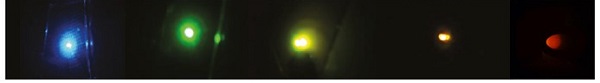
Figure 1. A full InGaN structure grown on InGaN-on-sapphire (InGaNOS) substrates can span the spectrum from blue to amber. (Source: Soitec) |
The advantages presented by microLED displays include low power consumption, high resolution, quick response and high luminance. In addition, sensors can be embedded within these displays. But there are still numerous challenges ahead for microLED technology such as cost, supply chain, defect management, mass transferability and efficiency. In particular, the efficiency of green LEDs remains a challenge. In addition, microLED displays require the use of red, green and blue (RGB) LEDs, achieved by mixing nitride LEDs and phosphide LEDs. This mixing causes blue, green and red LEDs to behave differently in terms of temperature and aging, which impacts image color quality. Moreover, blue, green and red LEDs each require specific electronic drivers, making integration more complex.
The ideal solution for microLED makers would be the availability of efficient nitride LEDs in both green and red. In this case, all RGB LEDs would be composed of the same material with the same behaviors and driving conditions. The challenge is to find one material capable of spanning the blue to red spectrum. Theoretically, the indium-gallium-nitride (InGaN) alloy can cover the entire visible range by adjusting the indium content to fine tune the peak emission wavelength. Unfortunately, high indium content in GaN-based LEDs results in poor quality because of lattice mismatches between the GaN buffer layers and the InGaN quantum wells.
An innovative material solution
To address these issues, Soitec has developed an innovative substrate called InGaNOX (InGaN-on-X) that overcomes lattice mismatch. The substrate has a top relaxed InGaN layer that can be used as a seed layer for full InGaN LED growth. The technology has been demonstrated in fabricating blue, green and red nitride emitting heterostructures on 100-mm wafers and is scalable up to 300-mm wafers.
The starting material is an InGaN donor template typically formed by a 200-nm thick InxGa1-xN layer atop 3-µm thick GaN on sapphire, in which the indium content x varies from 1.5 percent up to 8 percent. The InGaN layer is strained because of the lattice mismatch between GaN on sapphire and the InxGa1-xN layer.
The thin InGaN layer is then transferred using Soitec’s Smart Cut™ technology onto a compliant layer deposited on a substrate. Then the InGaN layer is patterned and all patterns are relaxed through a specific process developed by Soitec. To obtain final Ga-face polarity, a second transfer is performed onto the final handle wafer (figure 2).
 |
 |
|
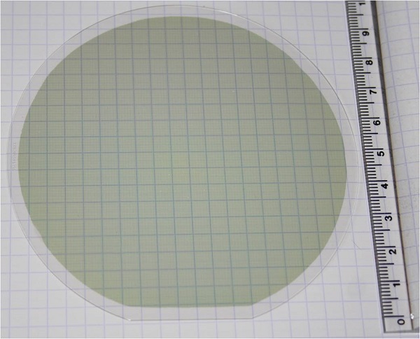
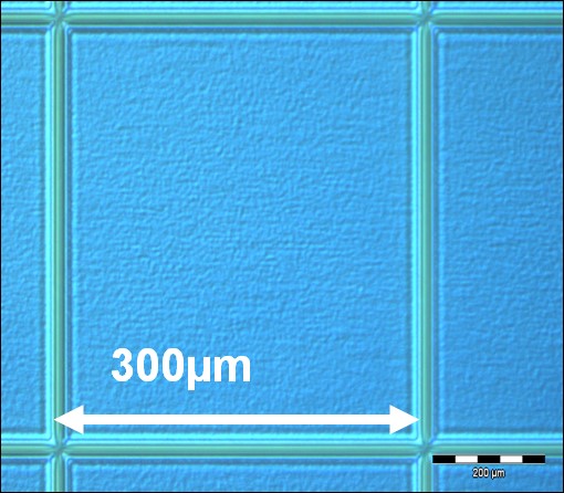
Figure 2. (a) A 100-mm InGaNOS substrate is shown with an In0.08Ga0.92N layer and 300µm x 300 µm patterns at 3.205 angströms. The brown area is the patterned In0.08Ga0.92N layer. (b) This microscopic view shows a 300µm x 300 µm pattern with a top partially relaxed InxGa1-xN layer. (Source: Soitec) |
Lattice parameters can be tuned from 3.190 angströms up to 3.205 angströms by the donor and relaxation process, enabling emissions from blue to red. Pattern size can be customized from square millimeters down to 5 µm x 5 µm.
This methodology is compatible with sapphire, glass or silicon handle wafers with sizes up to 300 mm.
Achieving green and red direct emission
The benefits of relaxed InGaN substrates are demonstrated by the growth of full InGaN emitting heterostructures and their direct emission. These heterostructures have been grown and characterized by the electronics research institute CEA-Leti.
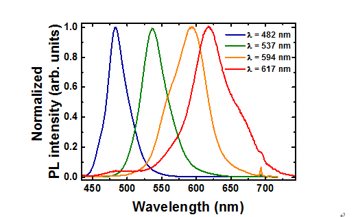
Full InGaN LED heterostructures composed of a ~200-nm InGaN buffer layer followed by 5x InxGa1-xN/InyGa1-yN quantum wells are grown on InGaN-on-sapphire (InGaNOS) substrates with lattice parameters from 3.190 angströms up to 3.205 angströms. The expected well and barrier widths are 3 nm and 8 nm, respectively. According to the lattice parameters of the InGaNOS substrate, indium incorporation varies in the InxGa1-xN wells for the same growth conditions. Emission from the heterostructure can be tuned from green (537 nm) to red (617 nm) with FWMH of 46 nm and 75 nm, respectively.
 |
|
Figure 3. Photoluminescence spectra at room temperature of full InGaN structures grown on InGaNOS 3.190 angströms (blue curve), InGaNOS 3.200 angströms (green curve), and InGaNOS 3.205 angströms (orange and red curves) are shown. (Source: Soitec) |
An InGaNOS substrate enables full InGaN heterostructures with direct emission from blue to red (figures 1 and 3), whereas standard green LEDs are the product of blue LEDs and phosphor conversion and standard red LEDs are made from phosphide LEDs. The next step is the fabrication of optimized full InGaN LEDs with external quantum efficiency (EQE) measurement.
A disruptive approach for microLED displays
Soitec’s disruptive technology solution addresses the major challenges facing the microLED industry:
- The substrates are suitable for producing high-efficiency green LEDs with direct emission, eliminating the need for phosphor converters.
- Color quality consistency is enhanced with full InGaN blue, green and red LEDs that do not require nitride/phosphide LED mixing.
In addition to producing high-efficiency and high-quality microLEDs, InGaNOX technology can be used to create substrates with mixed lattice parameters, enabling growth of different colored LEDs on the same substrate. This could drastically reduce the cost of microLED mass transfer for microdisplay fabrication.