No more packaging – Package-less Package. That is the fundamental solution which LED manufacturers are looking for to meet the market demands. Unfortunately, the era of Flip Chip-Chip Scale LED Package (FC CSP LED) is, however, emerging. It will make the time of the wide spread of LED light coming slowly step by step. Any LED manufacturers who aggressively jump over FC CSP LED and current leading-edge packaging technologies would be expected under the paradigm of no more packaging. A little of endeavour has been conducted to fulfil package-less package like Phosphor on Die and Package Free Chip.
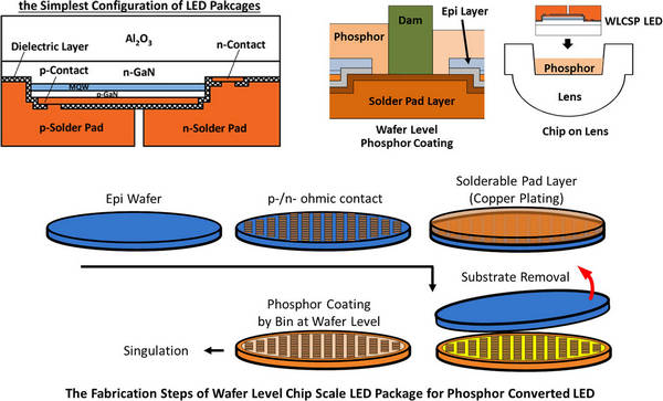
Wafer Level Chip Scale LED Package (WLCSP LED) is the solution of package-less package. Without any doubt the simplest configuration of LED package is to only form solderable pads directly on the LED chip without any other elements. WLCSP LED produces tens of wafers which have thousands up to ten thousands of LED packages formed directly on the epitaxial wafer by only forming the solder pads on the LED chips, while the existing LED packaging technology produces individual LED packages with LED chips diced from the epitaxial wafer.
One big challenge exists in WLCSP LED. That is Wafer Level Phosphor Coating (WL-PC) for Phosphor Converted LED (PC-LED) package. LED chips within the epitaxial wafer are grouped by bin, and phosphor must be coated differently by bin. Different phosphor coating by bin within wafer is impossible without affecting LED chip integration density. That is why phosphor is overflowed onto adjacent LED chips disposed densely on the epitaxial wafer.
Accordingly, WLCSP LED is to find a cost-effective technology about how to form different phosphor layer on the simplest structure of LED package by bin.
The following two ways overcome the challenge, keeping high chip integration density. One is WL-PC to form phosphor at the wafer level. The WL-PC requires a dam between LED chips which prevents phosphor from being overflowed onto the adjacent LED chips. The other is Chip on Lens (COL) that the singulated LED packages of the simplest configuration are grouped by bin, and then mounted on lenses of lens module as a phosphor layer is the adhesive between the LED package and lens. The WL-PC affects a little bit of LED chip integration density because of the dam width less than 50 micro meters. Like the Die Attach process, COL is independent on the fabrication of the simplest structure so that COL does not affect LED chip integration density at all.
As a result, WLCSP LED will be the cheapest LED package and have the simplest configuration of PC-LED packages. WLCSP LED with the WL-PC will be the smallest, thinnest PC LED package. COL will have the simplest fabrication steps. The copper plating layer of the solder pad can be thicker than 100 micro meters so that WLCSP LED can have high thermal performance. Moreover, the distance from LED chip to the solder pad on LED module PCB is shortest so that electrical impedance can be smaller and thermal performance can be higher.
As imagined, WLCSP LED will make LED packaging industry (its raw material industry as well) be restructured because it does not need any conventional packaging processes and LED chip manufacturers can produce WLCSP LED easier with much less investment than LED package manufacturers. It will be the risk of WLCSP LED, especially in the LED manufacturers vertically integrated from epitaxial growth and LED chip to LED package.
Nevertheless, it is believed that WLCSP LED will become the initiative to make LED light competitive against conventional lights in terms of their prices. Moreover, WLCSP LED will be suitable to all of the LED applications. Once LED package becomes far cheaper, new designs will come in LED module and LED lamp such as high voltage LED module with low or middle power WLCSP LEDs and modularized LED lamp. Emerging WLCSP LED in the near future would be expected, jumping over FC CSP LED.
(Author: Jin Sung Park, owner of Wafer Level Chip Scale LED Package)