An emerging landscape bereft of standards, some have defined Micro LEDs as anything where the LED semiconductor die is smaller than 70 μm down to perhaps 1μm. Larger die are typically called Mini LEDs, used in applications such as local dimming. The semiconductor die are essentially a miniature version of the die in the well-known, commoditized solid-state lighting (SSL LED) industry. Besides physical dimensions, there are some subtle differences between the SSL industry and the display industry. Spectral tuning notwithstanding, the end goal for SSL industry to emit “White” light, while displays requires full color (RGB).
Micro LEDs Features
-
They are far brighter than OLEDs per unit area. For a given display size, the emitter need not occupy the entire sub-pixel area. The brightness also allows for daylight viewability, critical for AR, HUDs, and various mobile devices.
-
They are power efficient. For a given device, the display power consumption can be substantially lower than an equivalent OLED or LCD screen.
-
They are comprised of inorganic materials and as such are impervious to moisture / oxygen (bane of OLEDs), so there is no need for encapsulation, nor generally a concern for lifetimes.
-
They can be switched very fast resulting in superior display performance compared to both LCDs and OLEDs. As displays get “smarter,” superior material qualities also allow for more built-in functionality, such as visible light communications (Li-Fi), sensors, detectors, etc…
-
They are self-emissive like OLEDs, however, do not suffer from now well-known “image sticking” and “burn-in” issues of OLEDs.
-
Finally, if the Mass-Transfer problem can be solved in a commercially feasible way, they can even be cheaper. A cheap 6-inch standard LED wafer (consider the excess production capacity of the SSL industry and existing infrastructure) can be sub-divided into MANY much smaller Micro LED dies, then re-populated over a much larger surface area, where each Micro LED die representing a sub-pixel of a larger display. For example, a single such wafer yields enough 10 μm die to populate 250 displays at 2 Million pixels each!
Displays also come in many different resolutions and sizes, depending on application. Billboard size video wall displays have differing needs than smartphones or wearable displays. The Micro LEDs that would form the emissive sub-pixels in these displays will be of different sizes; “Wall” sized displays could be made with mini dies, but for 4K or 8K high resolution “Wall” sized consumer markets micro dies would sooner apply. A Mass-Transfer technique that can handle smaller micro dies can be adapted to mass transfer of larger micro or mini-dies; however, the reverse is not true, it’s not always possible to scale a given method to mass transferring smaller micro dies.
Mass-Transfer Basics & Challenges
Mass-transfer here differs from mature, serial pick-and-place techniques in the semiconductor industry since many micro die must be moved simultaneously in massively parallel fashion, which can be further classified as deterministically (preserving orientation by design and intent), or stochastically (reorienting random die, e.g. through a fluidic process with external forces). The former is preferred since reorientation implies an associated cost. Deterministic Mass-Transfer involves three critical steps, typically done with some form of a “Transfer Stamp.”
The first step is picking-up micro dies (pre-made) from a predetermined location with very high spatial accuracy and orientation. Next step is to move these micro dies to a predetermined location while maintaining the relative spatial position and orientation of the micro dies. Then, selectively dispensing the micro dies at this new location while maintaining relative position and orientation.
The key Figures of Merit (FOM) in comparing different Mass-Transfer techniques may be the following:
-
Precision (how accurately can micro dies be moved onto the new location?), and depends on multiple factors: mass transfer technique, transfer stamp, and the fixtures used in the process.
-
Transfer yield: how many good dies can be successfully transferred at a time (of total transferred)?
-
Tack time: How many dies are transferred per unit time, or per unit transfer event?
-
Inspection method: provisions are made / possible to verify and confirm successful die transfer?
-
Critically and ALL IMPORTANT, does the mass transfer technique allow for repair and multiple transfers? Invariably some die will need to be re-oriented or re-positioned, repaired or replaced.
-
The range of the technique; i.e. the smallest and largest die transfer possible (recall the differing market needs and segments)?
Finally, cost of the process and tools, as well as intellectual properties of currently proposed deterministic processes are also critical.
Stochastic processes such as fluidic self-assembly with or without additional external forces as: acoustics /vibrations, electric or magnetic fields, self-assembly with physical, chemical templates and liquid/solid interfaces, and electrography are not discussed further; although massively parallel in concept, these processes have been investigated over the past few decades and while there has been progress, the levers for spatial manipulation of many micro dies in parallel are still limited, let alone issues with in-situ metrology.
A Proposed Solution
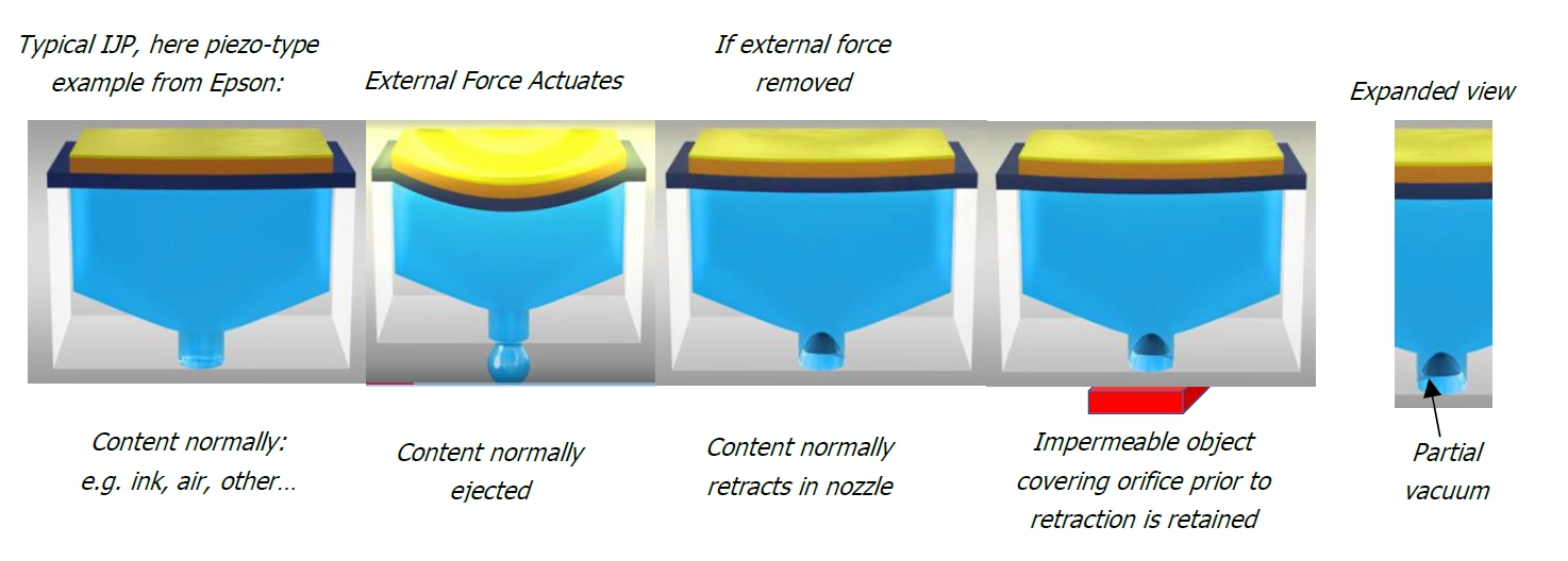
VerLASE is developing a very novel Mass-Transfer technique it has dubbed “Large Area Assembly Platform” or LAAP, based in part on cannibalizing technologies developed and perfected over several decades that are widely commercialized within several markets, Inkjet Printing in particular. The focus is developing systems ultimately allowing mass transfer of micro dies on the order of less than 10 μm, although first trials have been with larger die. The solution uses a form of Inkjet printheads, be they originally thermal inkjets or piezo inkjets, as transfer stamps, in a unique way to deterministically pick-up many micro dies, translate them to the desired drop-off location on a substrate and in an addressable manner deposit them with very high accuracy and speed.
Like today’s Inkjet printheads, the transfer stamp is also made in silicon, with additional MEMS features. Silicon was chosen to lever the vast silicon infrastructure and knowledge base available domestically and worldwide. Silicon properties are well characterized and consistent; existing foundries can shape and tailor it with very high precision at low cost. Standard processes widely used can create nozzles with exceeding small diameters, shapes, patterns, pitches, with sub-micron accuracy and repeatability at low cost. Cost of scaling, replicating and having a variety of SKUs is incremental, allowing for a wide variety of display patterns and pitches to be serviced.
A variety of micro die pickup modalities can be used, including partial vacuum, capillarity, electro-wetting, and others; the specific method used is proprietary. Dispensing can utilize gas and / or liquid droplet events. As example, one modality uses the pressure differential (resulting in partial vacuum) created in a system as it recovers from a partial evacuation event due to the displacement of gas / liquid inside the system after evacuation outside the system. Simplistically speaking, a pressure pulse is created in a nozzle with an orifice by actuating either a heating element or piezo element. This pressure pulse displaces some of the contents of the nozzle (gas or liquid) thru the orifice. As the pressure pulse dissipates, the remainder of the contents in the nozzle retracts back thru the orifice. If the entrance of the orifice is blocked by an impermeable micro die prior to the retraction event, the micro die is held in place at the orifice due to partial vacuum created inside the nozzle. This provides the suction force holding the micro die immobile, while a second pressure pulse can remove the conditions for partial vacuum thus releasing the micro die held at the orifice:
(Image: VerLASE)
Unlike conventional Inkjet Printheads, however, there is no ink refilling the nozzle post an ejection event. This is just an example of a highly proprietary process that doesn’t quite work so simply; other variants have also been anticipated for the pick-up and dispensing of the micro die, and the two steps need not be the same, but can be decoupled one from the other using different methods. Using the Inkjet printing paradigm, however, lets each of the nozzle elements be individually addressable.
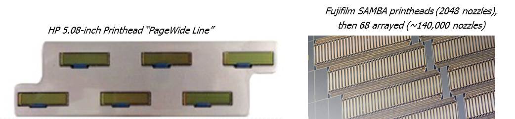
In current state of the art inkjet printing, it is common to multiplex a number of inkjet printheads side by side or staggered with respect to each other, allowing, for example, larger area printing, or fast single pass printing, etc. Some examples:
(Image: VerLASE)
Thermal Inkjet printheads with resolutions of 1200 PPI are available off the shelf. Assuming the use of such a printhead as a re-engineered transfer stamp, this translates to ~ 400 PPI for R,G,B full color display. To put this in some perspective, current smartphone display resolutions: iPhone 8, 326 PPI, iPhone 8+, 401 PPI, iPhone X, 458 PPI.
The central takeaway is that the platform as it currently stands can quickly be modified to service existing markets, and more importantly, scaled down to allow for even smaller microdies for even higher resolution in future products. As example, depending on transfer stamp layout and configuration, for a 2 x 2-inch square transfer stamp, transfers in excess of 10 million micro dies (square die <15 μm) per unit transfer event should be routinely possible.
Summary of the advantages
Author: George Powch and Ajay Jain/VerLASE