Why is it Important
Inorganic microLEDs are the next big thing in displays, not as backlights for LCDs, but like OLEDs, as the actual light emitting pixel elements, ranging from applications in Micro-displays for Augmented /Virtual Reality (AR/VR) to wearables such as Smartwatches and Cellphones. Unlike OLED displays, however, they are far more robust and long-lived, and most importantly, far more efficient and much brighter, making them viable even for larger displays, such as video walls in advertising and in cinema in place of projection. But to make the technology cost effective, manufacturing challenges abound, particularly as pixel sizes shrink in next generation micro-displays. For example, various coatings must be rapidly deposited in a precise, controlled manner, such as the Quantum Dots (QDs) integrated with the LEDs used in larger displays either to sharpen the color characteristics of traditional phosphors, or fully replace them in micro-displays, relying solely on QDs for color conversion. Better technology is needed for reliably depositing the various costly materials used, and even for rapidly assembling or arraying the microLEDs themselves.
QD films are also being used for color enhancement with LCD and OLED technologies, may ultimately be used in so-called QLED designs, and even used to enhance light absorption in cameras and photo-sensors (cf. QuantumfilmTM from Invisage, recently acquired by Apple). In all applications, rapidly and cheaply depositing these QD films and layers is critical. Moreover, in many applications the range of manufacturing challenges increases dramatically as pixel sizes shrink <20 µm. For example, in next gen VR / AR, micro-displays will evolve toward microLEDs: they are intrinsically some 103 brighter (hence so much more efficient) than the OLEDs currently being used, and are far more environmentally robust, a long lived, fully inorganic structure switching at semiconductor speeds (ns). Most importantly, they can be scaled in principle to the PPIs >1000 and sub-pixel sizes <<10 µm that will really be needed for next generation AR / VR, integrated with sophisticated optics to transfer an image onto a user’s field-of-view ...
But GaN /InGaN-based microLEDs are (with some exceptions) monochrome, typically blue/violet emitters, and must be down-converted to Green and Red for multi-color (RGB) or white light. This is typically done with phosphors for larger LEDs in lighting applications, but the column of phosphor material needed to fully absorb the blue makes them impractical for smaller pixel sizes (< 50 µm). QDs or other color converting approaches are therefore indispensable, playing an increasingly important role in displays in general, both in sharpening the spectral response of traditional phosphors, or altogether replacing them in display applications as pixels shrink << 100 µm … In all cases where QDs or other expensive nano-material coatings need to be laid down, however, there lacks a materials efficient process for quickly depositing precise, ultra-uniform films of such coatings, while ink-jet printing, spin or spray coating, slot-die or other relatively inefficient, costly approaches all have drawbacks.
Manufacturing Challenges
 |
|
(Image: VersufleX) |
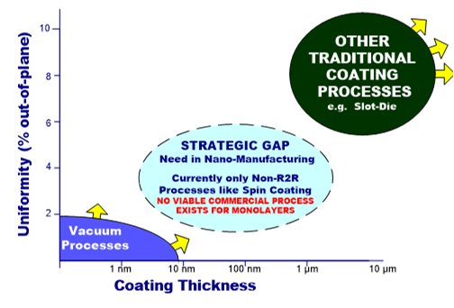
The major manufacturing issues and challenges in depositing QDs in such applications surround fine pitch pixilation, the practicality of dispensing over local vs. global areas, through-put, obtaining highly uniform QD coatings, and cost effectiveness; the various potential coating technologies summarized per the following chart:
While QDs are well-known, made off-site, and available from several vendors (Nanosys, Nanoco, ... etc), they are still relatively expensive, placing a premium on material efficient processes. They can be deposited in one of two ways: ink-jet printed with the appropriate color QDs at each pixel or blanket “printed” or spin-coated over the display area, then patterned by some form of lithography.
A fundamental challenge in either approach is controlling the loading density or number of QDs per unit volume, key for uniformity, the critical parameter (as with spin coating).
For low PPI and coarse demonstration purposes, ink-jet printing has been used, but is much too slow for volume production, especially for PPIs where sub-pixel sizes approach <10 µm, leaving areal deposition and lithography as the preferred approach. Some 7-10 µm or more thickness of a perfectly uniform QD coating is typically needed, with the QDs closely packed, to fully absorb the blue emitted by an InGaN LED, but the possibilities to do so are limited. Normal printing techniques are too coarse, while spin-coating limits to wafers, and wastes material. Indeed, spin-coating users typically cite some 80-90% of the coating materials wasted, not to mention edge-bead effects and the uniformity and packing issues tied to the centrifugal forces involved. Similarly, industrial slot-die processes are typically used for high volume coatings, but to achieve high uniformity, such techniques rely on precisely controlled evaporation of a diluent first dispersed into the material to be coated. Evaporation has many issues, not matter how well controlled, and such tools are expensive not only in capital, but also in the space needed for the drying ovens.
A Novel Solution ...
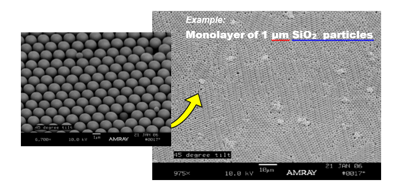
An approach experimented with by several University labs, called Linear Self-Assembly from VersufleX Technologies (www.versuflex.com), offers an intriguing solution. Precise, uniform coatings, down to nanoscale monolayers of particles become practical, in a higher speed web process and in air as the typical example below of 1 µm SiO2 particles illustrates:
 |
(Image: VersufleX)
|
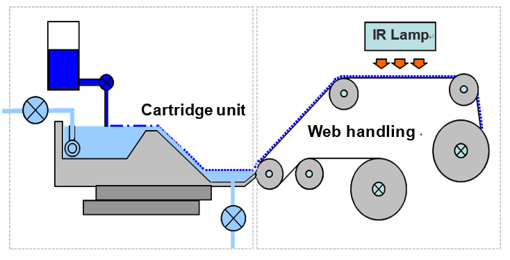
The operating principle automates the well-known Langmuir-Blodgett technique in a novel way: material to be deposited is put into a suspension, then dispensed in a precise, controlled manner onto the surface of a carrier liquid (e.g. DI water) of suitable density on which it “floats,” forming a bi-layer. The top layer is then made to self-assemble by inducing the bottom carrier liquid to flow, a function of dispensing and flow rates, surface tension and surfactants:
 |
(Image: VersufleX)
|
A “cartridge” unit with a precisely angled ramp between two carrier fluid ponds at different heights pumps the fluid at a controlled rate to form a closed, recirculating loop, and a web handling unit passes a moving substrate close to the lip of the lower pond. The controlled flow of the carrier fluid creates lateral pressure on the top layer causing it to self-assemble into a compact film or, if particles, into a monolayer:
 |
(Image: VersufleX)
|
The self-assembly process occurs on the surface of the ramp, dictated by the physics of the particles and fluids involved. The assembled layer is preserved down into the lower pond, then smoothly transferred onto a passing substrate over a colloidal bridge formed along the lip of that lower pond.
The coating thickness can be tightly controlled, with high uniformity of deposition, and multiple passes can be programmed for layer-by-layer (LBL) assembly for precise multi-level structures. Evaporation is NOT involved to reduce coating thickness, hence the process is also very energy efficient; any incidental traces of the carrier fluid, or of any other solvents, can be typically handled with IR lamps, as illustrated above.
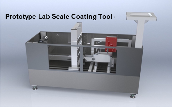
Several lab scale tools have been built and are in several university labs, typically in configurations with a 100-mm web (and delivery cartridge), roughly as illustrated, moving at 0-5 cm/sec ±0.1 mm/sec, although specialty fixtures can also handle wafers. The lab tools just use gravity for carrier fluid pressure through a reservoir of the carrier fluid (e.g. water) mounted on the elevated platform shown. Lateral surface pressure can be controlled 0-72 ±2 mN/m.
 |
(Image: VersufleX)
|
Applied to Depositing QDs
A wide variety of materials, liquid and particulate, in various sizes and shapes have been deposited with this technique for a variety of applications; there are some 40 recipes for coating different materials, being constantly expanded by university partners. QDs typically present suspended in an organic solution, with the identical challenges as with laying down ultra-thin polymer films (e.g. photoresists) for which the process is particularly well suited. After injection onto the moving flat fluid carrier layer, a polymer solution thins down in different ways, depending on the physical-chemical characteristics of the solvents and liquids used. The natural properties of the gas-liquid interface: flatness, mobility and tension, together with marangoni effects and gravity, hydro-dynamically drive the material at the interface toward and onto a film formation line. Pressure applied onto the film’s long axis is kept constant while the film is transferred from the liquid surface onto a solid substrate.
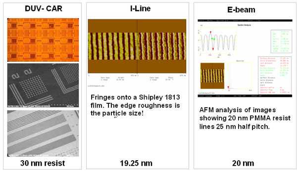
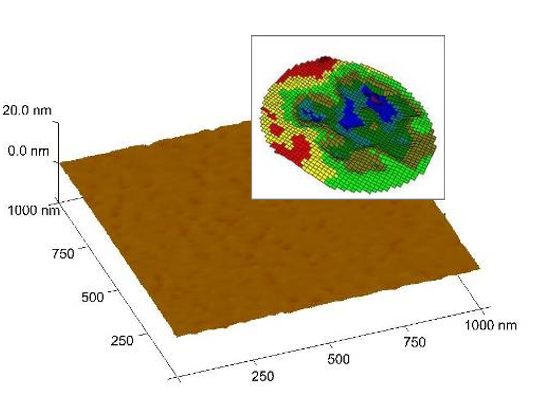
Following are some examples with common photoresists (SP1813, UV1400, AZ9260, NED, ZEP, and PMMA have been shown) and polymers for I-line, DUV and E-beam lithography, and an AFM example of 70 nm of UV1400 coated onto a 200 mm wafer with full thickness variation in the order of 1 nm and 0.2 nm Roughness as measured with MM-16 by Horiba:
 |
 |
(Images: VersufleX)
|
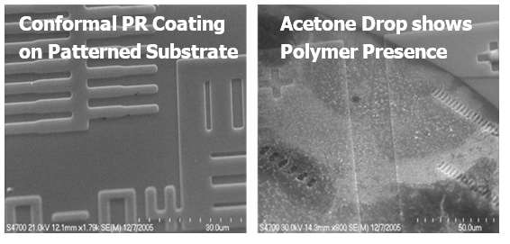
ltra-thin coatings are further highly conformal; shown below is a patterned substrate with a conformal resist coating compared to same with an Acetone Drop to show presence of polymer over the topography. But by varying the process parameters, the opposite can also be achieved: a suspended membrane over irregular topography, even a planarizing layer.
 |
 |
|
|
(Image: VersufleX)
|
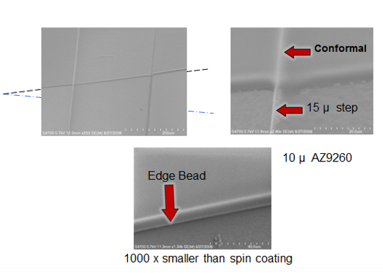
Above are magnified details of a 10 µm coating (typical of the QD thicknesses needed) of AZ9260 showing conformability across a 15 µm step, as well as the significantly smaller edge bead realized with this technique, when compared to traditional spin coating. The amount of expensive QD material saved with such a web process, compared to spin-coating can be significant. While it can produce coatings significantly better than state-of-art spin and spray coating, the focus is instead on new web (R2R) processes. For experimental purposes, wafers can also be handled, and/or fixtures designed for wafers in a production setting.
More Examples
The process is particularly well suited for particle monolayers, where no other known process is as fast or effective. A few examples:
 |
 |
(Image: VersufleX)
|
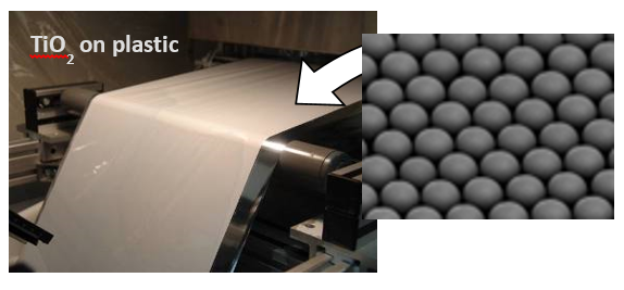
Adjacent to the above, uniform ordered layers of de-agglomerated nano-porous500 nm Ti02 particles deposited on aluminized plastic film on a 30 cm web based tool at speeds to 1.2 m/min. Porosity was controlled by the applied lateral pressure, varying 0-72.5 mN/m.
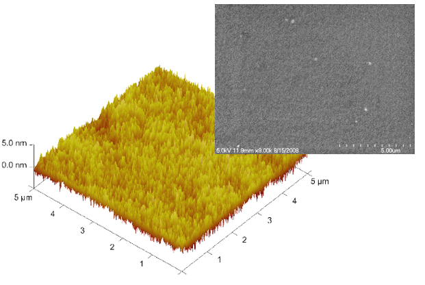
A multi-pass, 3 layer-by-layer stack of 5 nm Gold particles demonstrated for texturing of Poly-Si wafers as AR or reflective coatings, or texturing for SSL apps, and as a method for realizing photonic crystals and LBL assembly.
The dimensions of these particle are similar to those of QDs, which can be deposited either dispersed in a suitable host matrix /solution, or in a structured LBL as this example illustrates.
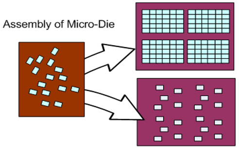
Finally, the process is a ready, fluidic means of rapidly assembling not only nanoscale particles, larger scale structures. These include structures such as micro-die, silicon slivers, nanowires … a number of applications are being explored, including assembling the microLED die themselves to predetermined patterns, in principle as illustrated as below:
 |
(Image: VersufleX)
|
VersufleX sells only the underlying tools to a patented process, with no claim on the applications to which the tools can be applied. Users are free to develop their own applications IP.
Summary
While MicroLEDs are far more robust, long-lived, efficient and much brighter than OLEDs, destined to become the next big thing in displays, particularly in Micro-displays for AR / VR applications and even Smartwatches and Cellphones, they have manufacturing challenges. QDs and various costly materials, must be rapidly and cost effectively deposited in a precise, controlled manner, but current technology may not be up to the task, particularly as pixel sizes shrink in next generation micro-displays. Better technology is needed for reliably depositing the various costly materials used. A new process called Linear Self-Assembly has been proposed, which effectively automates the well-known Langmuir-Blodgett process, transforming it from a R&D lab curiosity into a production worthy tool. A number of labs are actively developing applications for the novel process with lab scale tools from VersufleX Technologies (www.versuflex.com).
For depositing QDs, in particular, the choices for rapidly depositing ultra-uniform QD layers may be summarized as follows:
Major issues surrounding fine pitch pixilation, uniformity, the practicality of dispensing over local vs. global areas, and since QDs are relatively expensive, there is a large premium on material efficient processes. While processes such as ink-jet printing are fine for lab demos of coarse pitch displays, they are too slow for volume production, with issues as sub-pixel sizes approach <10 µm. Blanket deposition and lithography are preferred, but the major challenge is to obtain, successively and cost effectively, some 7-10 µm thick of a perfectly uniform QD coating to fully absorb the blue emitted by the InGaN microLEDs.
The proposed method has been proven to successfully deposit ultra-thin, ultra-uniform layers of polymer thin films, including advanced resists, PET, PEN, and monolayers of various particles, ranging from nanoscale to even assembling the microLED micro-die. The technology is further scalable to >30 cm widths at production rates to 4 m/min. It is ideally suited for rapidly laying down QD films.


