Despite the expectation of increased Mini LED penetration following Apple’s launch of its new iPad Pro, the production of such diode is still faced with several challenges. As we all know, transferring a tremendous amount of chips (a required step for Mini LED manufacturing, also known as mass transfer) using existing technologies and equipment is far too costly and time-consuming. As such, equipment providers have been striving for mass transfer solutions, making them crucial in the commercialization of Mini LEDs.
Stroke PAE, for example, performs Mini LED mass transfer using advanced technologies and has developed dedicated equipment. The company’s general manager Shao-Wei Huang agreed to an interview from LEDinside and shared how the company uses high-speed transfer solutions featuring high accuracy and yield to help its customers reduce cost and head towards mass production at a faster pace.

(Shao-Wei Huang, general manager of Stroke PAE; photo credit: LEDinside)
Stroke PAE Greatly Improves Mini LED Transfer Efficiency by Replacing Conventional Die Bonding with Unique Technology
With mass production of Mini LEDs being widely discussed, vendors have been rushing to propose various mass transfer tools and technologies. With their respective processes, each monitor, panel, LED package and mounting company has been launching relevant products.
However, as Huang indicated, most transfer equipment are still based on the conventional die bonding framework. When a conventional SMT is performed, substrates must undergo several steps including pre-bonding solder paste printing, SPI and post-bonding reflow soldering, all of which have unsolved challenges in different stages.
For example, the luminous uniformity of LEDs that have undergone reflow soldering can be difficult to manage due to their uneven surfaces. Huang specified that usually when a solder paste starts to melt, the flatness of LEDs can hardly be maintained, resulting in uncontrollable beam angles of the diodes after they cool down and become attached. This phenomenon is known as mura(which means “unevenness” in Japanese), indicating inconsistent luminous intensity. Having luminance consistency is extremely important for Mini LED RGB monitors because of its great influence on visual experiences.
Moreover, conventional die bonding approaches require the use of a reflow oven, which can easily lead to LED substrate warpage. Manufacturers tend to enhance the LED flatness by using thermoforming, but the process is costly for mass production due to the required time, accuracy and evenness.
Furthermore, die bonding machines transfer chips mostly with pick-up tools and swing arms. However, the mechanism does not work for all types of chips because of the limited size of pick-up tools. Huang specified that when it comes to the 0509 LED (5mil x 9mil, 127um x 228um) or even 0305 LED (76um x 127um), the pick-and-place yield and accuracy of a swing-arm die bonder will decrease considerably. The swing-arm design also generates a high level of static electricity, causing damage to the increasingly miniaturized Mini LED chips.
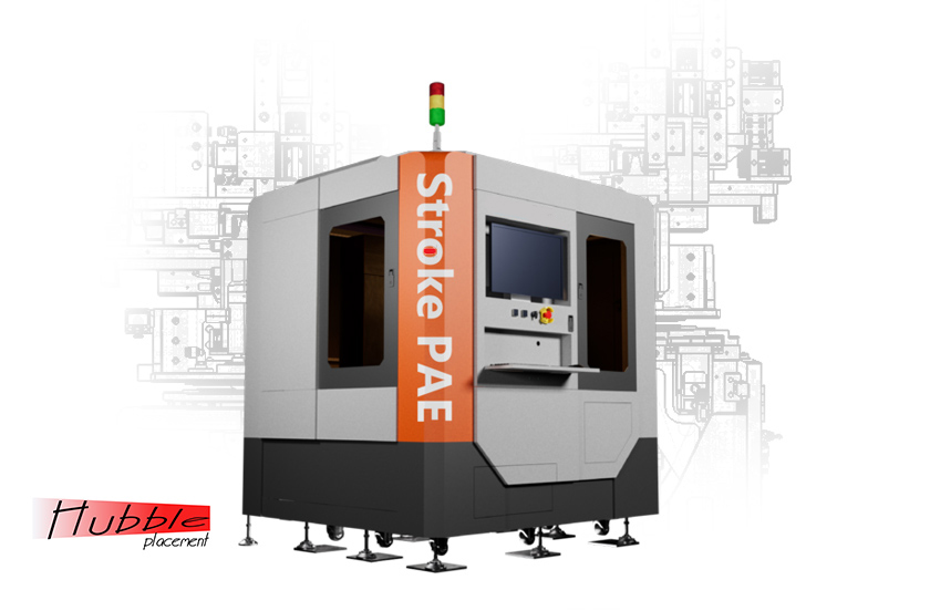
Overall, Huang revealed that the conventional die bonding process tends to significantly increase the difficulty of Mini LED production management with higher costs. To solve the problem, Stroke PAE developed a unique technology that enables Mini LED transfer with greater efficiency.
Reportedly, Stroke PAE’s unique technology can rapidly align Mini LEDs on a temporary substrate much faster than its swing-arm counterparts because of its customized design. Each module of the equipment can process more than 100,000 chips per hour (depending on the desired pixel pitch); the allowable chip size can be as small as that of the 0305 LED (accuracy = ±10um), with the chip-to-chip transfer edge distance being ≤40 um. Stroke PAE’s product can smoothly align and mount such small chips with much higher die bonding yield and accuracy, compared to swing-arm die bonders. Notably, Stroke PAE has managed to reduce the average bonding time to ≤10ms per chip by using its high-speed approach.
(Stroke PAE’s high-speed chip alignment machine HPP-180s; photo credit: Stroke PAE)
The biggest difference between Stroke PAE’s technology and conventional approaches lies in the chip alignment process. Stroke PAE adopts a unique mounting technique for die bonding rather than solder-based processes, thereby ensuring a high speed, high accuracy, and warpage-free process with desirable luminance consistency. Stroke PAE, in a wide variety of applications, offers different equipment for different customers, including those for Mini LED RGB products, Mini LED backlights , Mini LED packages as well as COB, POB and COG chips with highly effective solutions.
(Stroke PAE’s high-speed mounting machine NCB-156s; photo credit: Stroke PAE)
Rooted in Automation Equipment Manufacture, Stroke PAE Turns to Next Generation Displays Opportunities
As early as late 2016, the core team of Stroke PAE kicked off the research and development of Mini/Micro LED transfer technologies. The original goal was to develop a Micro LED process, as the chip fabrication technology and supply had yet to mature back then, prompting the team to instead focus on equipment for Mini LED transfer, mounting and repairs to satisfy customers’ demand.
Beforehand, the core team had long designed automation solutions for multinational brands and companies, providing them with customized automation equipment. Therefore, the team has sufficient know-how to develop equipment for Mini/Micro LED mass production, rather than just R&D machines.
(Stroke PAE’s mass transfer mounting machine MCB-156s; photo credit: Stroke PAE)
Unlike its competitors, whose development teams are mainly composed of staff from mechanism design and software departments, Stroke PAE has established an advanced process team to facilitate the development of equipment manufacturing processes and to gain a competitive advantage in mass production. The company also applied for various intellectual property rights, particularly patents, working together with the in-house electromechanical design and software development teams to realize an effective, real-time integration of core technologies and resources.
In 2018, the core team of Stroke PAE developed an experimental line featuring mass transfer equipment for fine-pitch Mini LED RGB and delivered it to its customer. In 2019, the team helped the customer upgrade the experimental line to a mass production line featuring high-speed chip alignment, mass mounting, optical inspection and LED chip repairs.
By extending its existing Mini LED technologies, Stroke PAE is currently striving for the development of Micro LED equipment, as the two technologies share some common ground. Huang emphasized that Micro LED was what Stroke PAE aimed at in the beginning. In 2017, the team already designed an optical inspection equipment for Micro LED production. Furthermore, due to its abundant experiences in manufacturing mass production lines of fine-pitch Mini LED RGB displays, Stroke PAE has gained the trust of leading display makers; the company was chosen as its partner in developing a Micro LED trial production line, consisting of chip transfer and mounting equipment as well as repair stations. This trial production line has already been established, ready for subsequent batch production.


