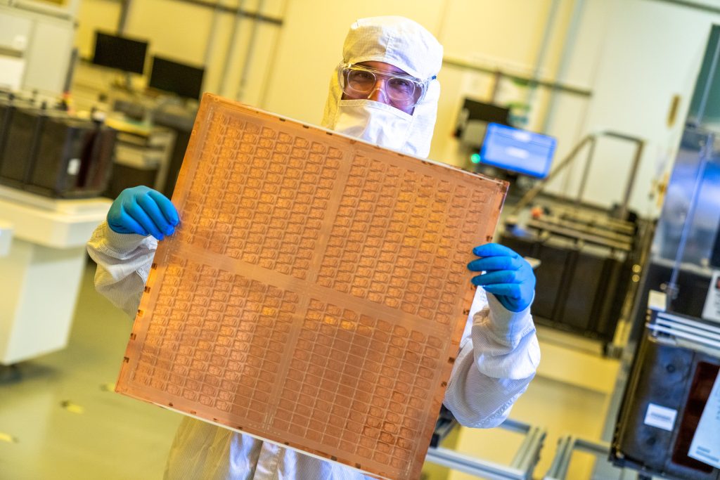
Intel has recently disclosed a patent originally filed in 2022, revealing an IC packaging architecture that integrates Micro LEDs.
The architecture features semiconductor dies embedded directly into a glass substrate, where Through-Glass-Via (TGV) within the substrate deliver power straight to the Micro LEDs on the dies. The power and signal connections are then routed to the mainboard via a package substrate.
According to the patent, the Micro LEDs can utilize nanowire structures to emit red, green, and blue (RGB) light. Potential applications include personalized decoration for DIY electronics, internal electrical testing indicators within the package, and illuminated lettering on the CPU surface, adding both functional indication and aesthetic appeal to the chip.
In terms of fabrication, through-holes and die cavities are created in the glass substrate using laser-induced etching followed by chemical etching. The TGV is then formed via copper electroplating, after which the dies with Micro LEDs are embedded into the cavities. Silicon nitride layers bond polymer package substrates on both sides, completing vertical interconnects for signals and power delivery.
The patent also details structural variations, including horizontal/vertical die placement and the integration of reflectors.
Intel has long invested in glass substrate technology. The company began researching glass as a replacement for organic substrates in 2013, accumulating extensive intellectual property before showcasing its first glass substrate samples in 2023.
Its commercialization efforts have accelerated significantly.
-
At NEPCON Japan, Intel displayed an engineering sample featuring a thick glass core combined with Embedded Multi-die Interconnect Bridge (EMIB) technology, achieving crack-free dicing on a large-format package measuring approximately 78×77 mm.
-
Later, at ECTC 2026, Intel presented high-volume manufacturing (HVM) technical validation for glass core substrates. This covered end-to-end process capabilities—including via formation, metallization, multilayer routing, and optoelectronic integration—highlighting defect-free 24-layer structures and precise warpage control.
Ecosystem collaborations are expanding as well. A wholly owned subsidiary of Lens Technology signed a Memorandum of Understanding (MOU) with Intel, prioritizing TGV advanced packaging as a primary area of joint development.
Under this partnership, Intel supplies architectural specs, Design for Manufacturability (DFM) guidelines, and validation methodologies, while Lens Technology handles via formation, high-precision laser processing, metallization deposition, and multilayer interconnect routing. Lens Technology has already delivered samples featuring millions of vias with a 0 ppm non-conduction rate to Tier-1 customers in North America and South Korea.
Additionally, Intel partnered with U.S.-based semiconductor technology company 3D Glass Solutions (3DGS) to advance a $3.3 billion glass substrate manufacturing facility in India. The planned facility targets an annual capacity of approximately 70,000 glass substrates, 50 million assembled units, and nearly 13,000 advanced 3D heterogeneous integration modules.
Designed to address high-density, large-format packaging requirements for AI chips and high-performance computing (HPC), the project is slated to begin high-volume shipments between 2028 and 2030.
(Photo credit: Intel)
TrendForce 2026 Micro LED Display and Non-Display Application Market Analysis
Release: 15 September 2026
Format: PDF
Language: Traditional Chinese / English
TrendForce 2026 Infrared Sensing Application Market and Branding Strategies
Release: 01 January 2026
Format: PDF / EXCEL
Language: Traditional Chinese / English
Page: 168
|
If you would like to know more details , please contact:
|


