Epitaxy wafers are key to the technology development of Micro LED displays. As Micro LED chips are extremely small, the quality of epitaxy wafers including wavelength uniformity and low defect becomes critical for further production process.
AIXTRON, the German-based technology company, has illustrated how its MOCVD systems can significantly improve wavelength uniformity and decrease defect density of Micro LED epitaxy wafer with its article, titled “AIXTRON’s MOCVD Technology Breakthrough for Micro LED High Volume Manufacturing.” As the article focuses on the fundamental issue of Micro LED epitaxy processing, it was selected as the winner of the Micro LED Technology Research Contest.
LEDinside was honored to have an interview with Arthur Beckers, Senior Product Manager at AIXTRON, to learn how its equipment plays an essential role in the Micro LED manufacturing process and how the company positions itself in the development of Micro LED technology.

(Interviewee: Arthur Beckers, Senior Product Manager at AIXTRON; Image: AIXTRON)
How AIXTRON accelerates Micro LED technology development
AIXTRON has recognized that Micro LED technology, as the next generation display technology, is opening a new horizon of consumer products with its low power consumption and excellent pixel density to perform high brightness and display contrast. Beckers addressed that large size TVs sized from 75-inches and larger is the sweet spot for Micro LED display technology while Augmented Reality, Head-up displays and Smartwatches have great potential as next-gen Micro LED display product by delivering the mix of ultra-high brightness, small form factor, low power consumption and potentially also lower cost.
With the acknowledgment of its technology, AIXTRON stands at a unique position to provide the only viable MOCVD solution for enabling the High Volume Manufacturing (HVM) of these Micro LED products, highlighted Beckers.
Why is AIXTRON proud of its technology? Beckers noted that the miniaturization of LED chips imposes a strict requirement for Micro LED wafer on both cost and quality. Before entering into Micro LED processing it is required to reliably demonstrate an extremely high level of wavelength uniformity. That is, a wavelength range specification of less than 4nm overall. This is the key to enable displays with the required color accuracy. On top of that the MOCVD system must accommodate for producing with the lowest defect and particle levels. Beckers addressed that AIXTRON is working based on a 6-inch specification, which equates to less than 0.15 defects per square centimeter.
Aside delivering extreme good quality the system needs to be designed to reduce and control cost as well. The key cost influencers are found in eliminating sorting and reduction of pixel repair as well as increased wafer size for better stamp transfer yields. As a result, the MOCVD system needs to deliver an unmatched production yield in a HVM mode.
Many might consider that the existing equipment for conventional LED wafers could be easily modified for Micro LED. Unfortunately, it is not as simple as it may seem. To clarify the misunderstanding, Beckers stressed that for Micro LED technology, “The industry is running against the ‘Wall’ as long as conventional equipment is utilized. This is where AIXTRON can offer its partners the unique Planetary® technology to overcome barriers and meet these high-level industry requirements.”
Technology breakthroughs of AIXTRON’s MOCVD systems
With the purpose to offer cost-effective MOCVD equipment to accelerate Micro LED adoption, AIXTRON illustrated how its systems are suitable for the increasing requirements of the Micro LED industry for wavelength uniformity and low defect density.
The Planetary Reactor® technology with Gas Foil Rotation® (GFR) is a hybrid solution combining single wafer rotation and batch reactor processing. A satellite to satellite control function uses GFR to allow individual wafer temperature control and flow tuning, explained Beckers.
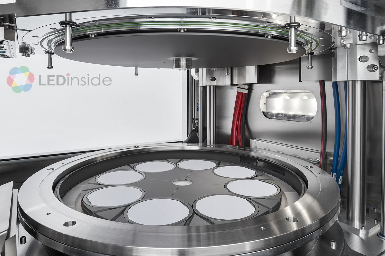
(AIX G5+ C, Planetary Reactor®, 8x6” configuration; Image: AIXTRON)
As for reducing the defect level, Beckers mentioned that by executing in-situ reactor cleaning and using a cassette-to-cassette system for wafer handling, AIXTRON’s customers have confirmed to meet the required defect and particle levels.
Currently AIXTRON has two platforms, AIX 2800-G4 TM and AIX G5+ C, in place to address the MOCVD production of the three primary colors, respectively RED and BLUE, GREEN. These platforms are today’s tool-of-record and proven for advanced LASER, VCSEL, HEMT and RF applications and are state of the art manufacturing tools for Micro LED as well.
AIXTRON’s market strategies and prospect of Micro LED technology
AIXTRON, as the provider of the only viable MOCVD solution, is working closely with key players in the industry. In order to perfectly match the demands of Micro LED technology adoption in consumer products, AIXTRON has been continuously engaged with LED chip producers. Furthermore, Beckers reveals that AIXTRON also stays in contact with its indirect clients such as display makers, to fully understand their requirements for Micro LED productions and advance its equipment for meeting the needs of the end products. The key to becoming a successful equipment developer in the industry is to keep listening to the manufacture chain and integrate the requirements into solutions.
As for the development timeline of Micro LED products, AIXTRON believes that it would take up to two or three years for Micro LED technology to become cost competitive for consumer products like large size TVs. Other Micro LED display applications may become cost competitive after that. Beckers pointed out that more innovation and effort are needed in the manufacture chain to solve the current challenges. He underlined, “High volume manufacturing capability requires a shared industry roadmap to allow a balanced integration of the manufacturing steps and to accelerate Micro LED adoption.”
Currently, AIXTRON’s MOCVD solution target 6- and 8-inch Micro LED epitaxy wafers. Beckers states that AIXTRON is engaged with a broad field of Micro LED manufacturers and has demonstrated its performance level with the AIX G5+C for both ‘GaN-on-Sapphire’ as for ‘GaN-on-Si’. Samsung LED is one of these renowned AIX G5+C users for GaN-on-Si LEDs. They are one of the players who have acknowledged the G5+ system performance demonstrating excellent results. Also AIXTRON recently announced that its MOCVD customer Plessey Semiconductors purchased an AIX G5+C for GaN-on-Si applications like monolithic integration of Micro LEDs.
As for every process which can be done on Silicon, the question about market evolving towards 300mm is coming up from time to time. “We believe that it may eventually come but is far down in any roadmap, since beyond technical feasibility, the projected cost gain by switching to 300mm would need a very large invest and epi volume to realize – which are not seen today”, said Beckers.
Comments from the Judges on the Articles
Judges at the Consortium for intelligent Micro-assembly system (CIMS) at ITRI appreciated how AIXTRON’s MOCVD solutions manage to target the two key issues of epitaxy production in the Micro LED industry. As these two factors are influential to cost control and yield rate improvement in further Micro LED manufacturing processes, advancing the essential MOCVD equipment technology will help to accelerate the commercialization of Micro LED.
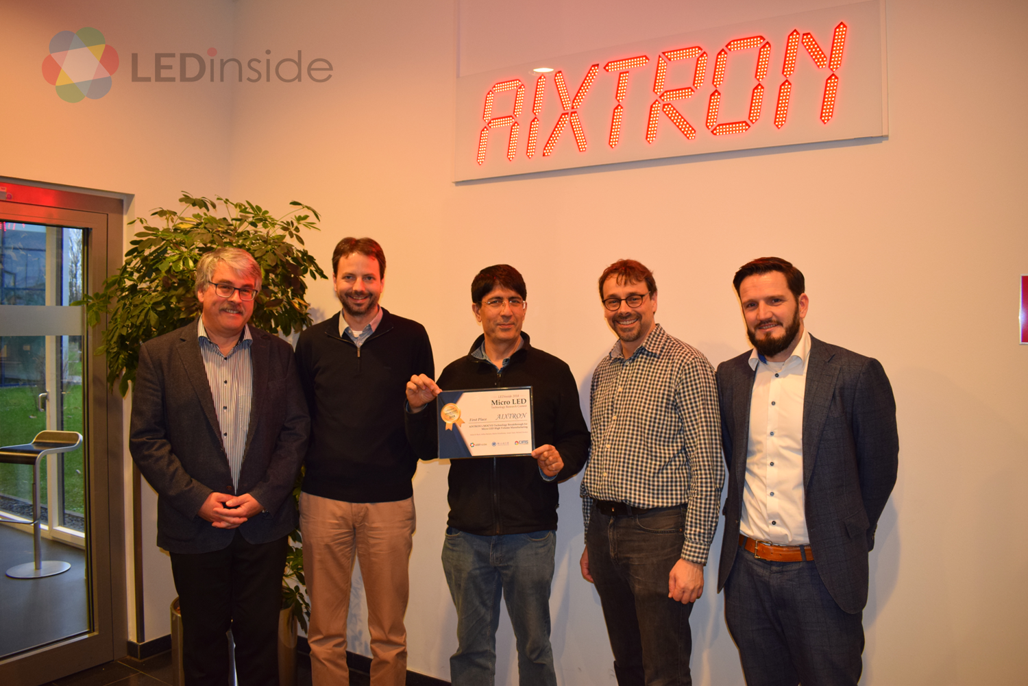
(authors AIXTRON Team holding ‘Micro LED Technology Research Contest award; Image: AIXTRON)
See full paper: AIXTRON’s MOCVD Technology Breakthrough for Micro LED High Volume Manufacturing


