Narendra Mehta, Senior Power Management Systems Engineer at Texas Instruments shares some of his insights on how to use GaN power driver designs in this latest blog entry.
You may have recently encountered “GaN,” which is replacing silicon (Si) in some key applications for power conversion. In this blog series, “How to design with GaN,” I will take a look at how gallium nitride (GaN) is different from Si and what the key considerations are when creating a power design with GaN.
Awhile back, I started working on the definition and evaluation of the LMG5200, which is a GaN half-bridge field-effect transistor (FET) with an integrated driver. What are its advantages? Higher efficiency, reduced form factor, new applications – the list goes on. On my first day working with this new device, I realized that we were dealing with something totally out of the box. A material so fast that the old techniques of designing power boards needed a thorough revisit, a back-to-the-whiteboard methodology.
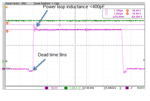
It became clear that to get the best performance out of this device, I could not just simply replace the silicon half bridge with the LMG5200. I had to optimize the power loop to ensure that the entire power-loop inductance is in the order of 400pH or less. This meant using inductance-cancellation techniques by ensuring that the return path was directly underneath and as close as possible, using decoupling capacitors with low inductance in addition to the bulk capacitors for the bus.
Low power-loop inductance minimized the amount of overshoot and ringing in the switch node (Figure 1). This helped with efficiency and also avoided any chance of violating the device’s absolute maximum ratings (see here).
This application note on layout techniques delves into the details of how to optimize the power-loop layout.
|
|
Figure 1: Switch node (channel 3) shows minimal ringing and overshoot. |
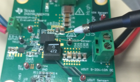
Measuring the performance of GaN devices also required special considerations. I had to keep the probe ground as close as possible to the switch node, as shown in Figure 2.
 |
|
Figure 2: Using a small pigtail for ground ensured that the measurement loop was small and gave better results. |
To maximize the benefits of a GaN half bridge with an integrated driver like the LMG5200, it’s important be extremely mindful of the power-loop inductance to get the highest performance.
In the next post of this series, I will continue to explore the benefits that the LMG5200 provides compared to Si power FETs, as well as discrete GaN devices.


