Micro LED technology builder VerLASE introduced a novel mass transfer technique for Micro LED display production based on its “Large Area Assembly Platform” (LAAP), which the company revealed in June, 2019. With similar concept, the company transfer the technology into a simpler, semiconductor-fab compatible solution based on Photo-Mechanical Actuation (PMA).
According to VerLASE, the solution uses a novel formulation comprising of fab compatible chemistries and transfer stamp architecture in a unique way to deterministically pick-up a large number of microdies, translate them to the desired drop-off location on a substrate and then dispense them with very high accuracy and speed. This microdie dispensing can be done globally or locally by individually addressing microdies, as programmed.
Simplistically, the Transfer Stamp follows a 3-ply construction: a thin transparent substrate, a patterned PMA formulation, and a stiffer material dubbed “Barrier Ribs” surrounding the patterned PMA formulation as illustrated below:

(Image: VerLASE)
The substantially transparent and flexible Transfer stamp allows for accurate alignment with the donor LED source wafer and the microdies held on it, as well as the receiving target interposer or display backplane.
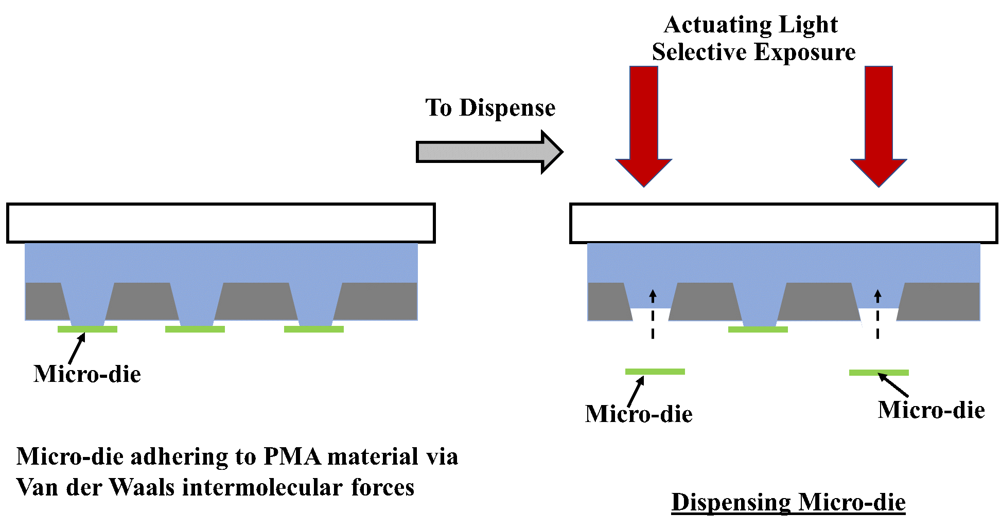
VerLASE noted that the solution can work with different ways to pick up the microdies while it used a proprietary method. And the dies dispensing is accomplished by either flood or selective exposure of the PMA material in the Transfer Stamp to light. The novel photo-reactive chemistry undergoes light induced physical contraction under illumination by a light source.
As the PMA material contracts under this light illumination pulling the attached microdies with it, the “Barrier Ribs” act as a hard, physical stop forcing the bonding interface holding the microdies to the PMA material to give way, thus releasing the microdies. The bonding strength of the microdie / PMA material interface can be varied as necessary such that it is low enough for detaching the microdie without the microdie structurally failing.
Existing exposure tools coupled with binary chrome photo masks and scanning low power laser systems allow for a highly multiplexed, addressable mass release of microdies or local dispensing of microdies as desired.
(Image: VerLASE)
PMA material formulations being investigated at this time are Photo-Actuated, primarily single use chemistries, but other options could also be applied with future development.
A full wafer transfer stamp as illustrated above, scalable to 6 inch or larger, can be constructed with existing tooling with very high precision at low cost. Cost of scaling, replicating and having a variety of SKUs is incremental, allowing for a wide variety of display patterns and pitches to be serviced.
Furthermore, the Transfer stamp, once constructed, can be mated and used with minimally modifying existing, semiconductor equipment. The full wafer transfer stamp should allow for the mass transfer of microdies on the order of less than 5μm.
As a full wafer transfer stamp and at microdie sizes of less than 5 μm, transfer rates in excess of over 10 million microdies per unit transfer event should be routinely possible, enabling a wide variety of display resolutions and display sizes to be economically manufactured.
VerLASE expects to produce displays with above 400 ppi for smartphone sizes with the method which achieves high thruputs and with provisions for in-line metrology and in-process repair.
Aurthor: George Powch and Ajay Jain / VerLASE; edited by Yining Chen / LEDinside


