The upcoming LED technology will be GaN-on-GaN LEDs, affirmed Nobel Laureate in Physics Shuji Nakamura and fellow colleague at University of California, Santa Barbara (UCSB) Professor Steven DenBaars at an exclusive forum hosted by Taiwanese leading chip LED manufacturer Epistar on Wednesday at the company headquarters in Hsinchu, Taiwan.
(For those unfamiliar with Nakamura’s rock star status in the LED and lighting industry, the bottom section of this article gives an overview of the birth of blue LEDs.)
 |
|
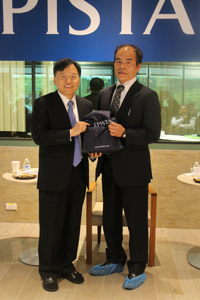
Left to right: Epistar Chairman B.J. Lee and Shuji Nakamura, Nobel Laureate in Physics and UCSB professor. (LEDinside) |
Nakamura and DenBaars: Forget about GaN-on-Si LEDs!
LED technology has rapidly developed since the first GaN on sapphire LEDs hit the market in the 1990s. Manufacturers have been raising the energy efficiency of GaN LEDs over the years, raising it to about 300 lm/w last year. However, the efficiency of GaN on sapphire is nearing a peak, as improvements in energy efficiency have gradually slowed in recent years. Droop remains the major technology challenge for GaN on sapphire and to overcome this, manufacturers would have to push droop to 100 to drive the sapphire five to six times harder, said DenBaars.
In addition, sapphire costs has led LED manufacturers to search for alternative solutions. Two different technology approaches have emerged, one being GaN-on-Si to drive down LED costs, and the other GaN-on-GaN developed by UCSB research team, which aims to deliver higher performing LEDs.
Responding to the future of GaN-on-Si LEDs, DenBaars said without hesitation: “I think it is a waste of time.” Analysis by Phlips Lumileds and Strategy Limited have indicated there was no cost advantage for it over GaN on sapphire LEDs, he explained. This view was also shared by Nakamura, who urged the industry to focus on GaN-on-GaN technology. “GaN-on-GaN, only one girlfriend,” he said. He also challenged industry experts to aim for the “ultimate technology.”
GaN-on-Si material first emerged in the semiconductor industry in 1970s, but only a few LED manufacturers including Toshiba and Samsung are investing heavily in this technology. Silicon wafers cost less than sapphire, but high lattice mismatch between GaN and silicon result in higher defect density rates in epitaxal layers. Moreover, the substrates often bend, or warp in semiconductor language. GaN-on-Si wafers bend in the growth process as it cools down at room temperature because of the high thermal expansion coefficient (TCE) mismatch between GaN and silicon.[1]
In the near future, GaN-on-Si might not be the solution for LEDs, but DenBaars envisioned the technology might have a good chance in drivers. This could be achieved through vertical integration manufacturing, said DenBaars, who’s research is also in high power devices. Power devices are often grown on silicon, added Nakamura.
 |
|
Steven DenBaars, Professor at UCSB and co-founder of Soraa. (LEDinside) |
GaN-on-GaN LEDs the future of LED technology
Nakamura and DenBaars urged for GaN on sapphire manufacturers hitting the efficiency ceiling to invest in GaN-on-GaN research, upholding this as the ultimate LED technology and the next viable option was laser (which we will address in a separate article).
The advantages of GaN-on-GaN LEDs include its substrate structure and efficiency level. GaN substrates facilitation rates is much lower than GaN on sapphire, and its current density is five times higher than sapphire, said Nakamura. According to info published by Soraa, the company Nakamura and DenBaars co-founded, the LEDs have an efficiency closer to laser, which translates to lower droop than conventional LEDs.
Costs is the biggest stumbling block for the development of GaN-on-GaN LEDs. GaN substrates are very expensive, and can be four to five times higher than sapphire, said DenBaars. To overcome this, the UCSB research team has been testing ammono-thermal technology to grow GaN crystals, but costs remain high. Instead costly Hydride Vapour Phase Epitaxy (HVPE) crystal growth methods are used, said Nakamura. Yet, Nakamura remained optimistic that ammono-thermal GaN crystal growth methods would be the answer to driving down substrate costs in the future, it would be possible to grow 4-inch, 6-inch and 8-inch GaN wafers in the future, added Nakamura. The research team is also testing growing GaN on different crystal planes to create semi-polar LEDs to see if it can drive down costs, said DenBaars.
GaN-on-GaN is good for directional lighting applications where high brightness and density is required, such as MR16 LED lamps, explained Debaars. In the meantime, before GaN-on-GaN fully takes off, manufacturers are unlikely to ditch good old sapphire substrates because of the cost advantages it has over both silicon and GaN substrates.
LiFi and UV LED might be industry next killer app
Asked about the next major application for LEDs, the two LED experts did not pin point UV LEDs. Sure, UV LEDs would remain promising in the medical sterilization and detection industry, where there could be big area for growth, said DenBaars. The sector was, however, attracting a lot of competition as more manufacturer aim to join, he observed. As for UV technology barriers, UVC efficiency is very low, and there needs to be a big breaktrhough to reach better efficiency, explained DenBaars.
LEDs in communication applications could be the next big thing, such as LiFi. In U.S., there has been 20 new LiFi startups over the past year, said DenBaars. Modulation has not been fast enough, but if LiFi picks up it could be a killer application. LiFi signals, which rely on LED light transmission, are known to be more secure than traditional WiFi signals.
The future trend for LED technology will be in GaN-on-GaN from DenBaars and Nakamura’s perspective, and niche markets such as LiFi and UV LED might be the answer for manufacturers searching for a new direction.
 |
|
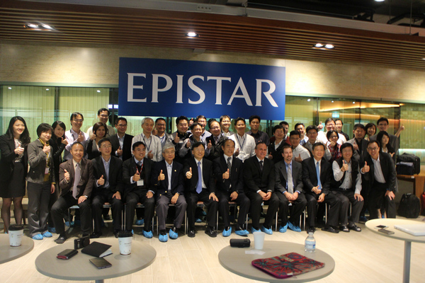
All attendees at Epistar's exclusive forum featuring Professors Shuji Nakamura and Steven DenBaars. (LEDinside) |
Birth of blue LED walkthrough
Nakamura started researching on GaN material in 1988, when he was a Nichia Chemical employee. Back in the day, it was difficult to create high quality GaN crystals, since most of the industry thought it was not worthwhile to build a surface for GaN crystals. Even though GaN was recognized as a blue light material in the industry, it was considered nearly impossible to build p-type layers on the material[2]. DenBaars, who was working as a technical staff at Hewlett-Packard's Opkoelectroncis Division at the time, recalls LED expert George Craford, who was the division leader then, told him to drop GaN LEDs. Most experts in the LED industry were betting on II-VI semiconductor material, such as zinc selenium (ZnSe) at the time, explained DenBaars.
To overcome some of these technical difficulties, Nakamura built two MOCVD equipment in 1990 to meet the challenge of creating high quality GaN. Eventually, he developed a GaN LED technique that was much more cost effective from Akasaki and Amano. The method he developed in 1992 was growing a thin layer of GaN at low temperature first, and growing subsequent layers at higher temperatures. By heating the GaN material Nakamura was able to create a functional P-type. In contrast, Professors Isamu Akasaki and Hiroshi Amano of Nagoya University, Japan, developed their first high-quality gallium nitride crystal in 1986 by growing high quality GaN on top of a layer of aluminium nitride on the sapphire substrate. They created a p-type layer by the end of the 1980s, and presented the first functional blue LED at around the same time as Nakamura.
The three Japanese scientists’ breakthrough in gallium nitride (GaN) material broke a 30 year LED technology impasse of making highly efficient blue LEDs. By overcoming the GaN technology barrier, their work in blue LEDs finally paved the way for the emergence of white lights, which is created by mixing red, blue and green LEDs. This significantly broadened the application of LEDs, and brought LEDs from backlight applications to general lighting market. (For more info please see here.)
In 2000, Nakamura resigned as head of Nichia R&D to become a professor at the College of Engineering at UCSB. Together with fellow UCSB professors DenBaars and Jim Speck, the three later went on to co-found LED company Soraa in 2008. DenBaars is a veteran in the LED industry, having accumulated extensive experience in fabrication of visible LEDs at HP from 1998-1991. He later received a NSF Young Investigator award in 1994, and the IEEE Fellow award in 2005. Working on the same research team as Nakamura, DenBaars research interests are in wide-bandgap semiconductors (GaN based), and application in blue LEDs, lasers and high power devices.
Since inventing the blue LED in 1993, Japanese media have been anticipating the day he would become a Nobel Laureate, said Nakamura. They had been waiting on his doorsteps patiently for 20 years for the announcement.It was not until 2014 that Nakamura, Akasaki and Amano was jointly awarded a Nobel Prize in Physics for their invention of blue LEDs. For some reason, the Nobel Prize Committee made no mention about InGaN, noted Nakamura. “I was actually very depressed when they announced the prize because they made no mention of InGaN,” said Nakamura. InGaN was the key to making high efficiency LEDs, he added.
(Author: Judy Lin, Chief Editor, LEDinside)
References:


 CN
TW
EN


