Zoé Pál Bőle from Texas Instrument (TI) shares in this blog entry the benefits of using GaN trasnsitors for high-speed motor drive applications compared to conventional silicon transistor technologies.
Unlike switched-mode power supplies, three-phase motor-drive inverters generally use low switching frequencies; only a few tens of kilohertz. High-power motors were large with high inductance windings; therefore, the current ripple was acceptable even with a low switching frequency. With advancements in motor technology, power densities have increased; motors are built in smaller form factors and designed for higher speed, which requires a higher electrical frequency.
Low-voltage brushless DC or AC induction motors with low stator inductance are increasingly or exclusively used in precision applications like servo drives, CNC (computer numerical control) machines, robots and utility drones. To keep current ripple within a reasonable range, these motors – given their low inductance – require switching frequencies up to 100kHz; phase-current ripple is inversely proportional to PWM (pulse width modulation) switching frequency and translates to torque ripple in mechanics, which creates vibrations, reduces drive precision and decreases efficiency.
Then why don’t engineers simply increase the switching frequency? As always in engineering, it’s a compromise. The inverter’s power losses mainly comprise conduction losses and switching losses. You can reduce switching losses at a given operating frequency by downsizing the switching elements (usually MOSFETs), but this leads to increased conduction losses.
In an ideal design, the highest achievable efficiency is limited by the technology of the semiconductor switches. With a traditional low-voltage 48V silicon MOSFET-based inverter, the switching losses at 40kHz PWM may already be significantly higher than the conduction losses, and hence dominate the overall power losses. To dissipate the excess heat, a larger heat sink is necessary. Unfortunately, that increases system cost, weight and total solution size, which is undesirable or unacceptable in space-constrained applications.
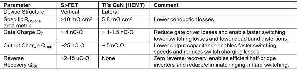
Gallium nitride (GaN) high-electron-mobility transistors (HEMTs) are opening new possibilities by having several advantages over silicon MOSFETs. GaN transistors can achieve a much higher dV/dt slew rate, and thus can switch much faster than silicon MOSFETs, significantly reducing switching losses. Another advantage of GaN transistors is the lack of a reverse-recovery charge, which causes switch-node ringing with traditional silicon MOSFET designs. Table 1 compares silicon FETs and GaN FETs.
 |
|
Table 1: Comparison between silicon power MOSFETs and TI’s GaN FETs (HEMTs). (All images courtesy of Texas Instrument) |
The world would be too easy if you could just swap the existing silicon MOSFETs with the new GaN FETs and enjoy the benefits. For example, achieving high slew rates poses unique challenges in gate-drive circuitry and printed circuit board (PCB) layout. If handled improperly, higher dV/dt means increased electromagnetic interference (EMI). The propagation delay mismatch between channels will limit the best achievable dead time, preventing the GaN FETs from achieving their optimum performance.
TI’s LMG5200 GaN power stage overcomes these difficulties by integrating two 80V/10A 18-mΩ GaN FETs with gate drivers in the same bond-wire-free 6mm-by-8mm quad flat no-lead (QFN) package. The package’s pinout is designed for low power-loop impedance with easy PCB layout. The inputs are 5V TTL and 3.3V CMOS logic-compatible, and have a typical propagation delay mismatch of 2ns. This enables a very short dead time, which reduces losses and output current distortions.
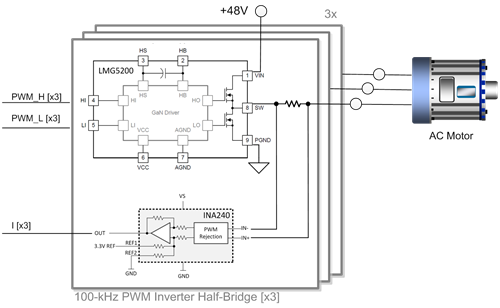
The TI Design 48V/10A High Frequency PWM 3-Phase GaN Inverter Reference Design for High-Speed Drives realizes a B6 inverter topology with three LMG5200 half-bridge GaN power modules. Figure 1 shows a simplified block diagram. This reference design offers a TI BoosterPack™ module-compatible interface to connect to a C2000™ microcontroller (MCU) LaunchPad™ kit for easy performance evaluation.
 |
|
Figure 1: High frequency three-phase GaN inverter reference design. |
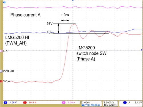
After so much theory, are you curious as to how fast you can switch in practice? Figure 2 shows the switch node with a slew rate of around 40V/ns. Despite the ultra-fast switching, the switch-node overshoot is less than 10V. Unlike traditional silicon FET designs, this requires less headroom between the FET’s VDS breakdown voltage and the maximum permissible Vbus supply voltage.
 |
|
Figure 2: Switch node at a 48V input and 10A load. |
The very high slew rate makes shunt-based in-phase current measurement also challenging. The 48V 3-Phase Inverter with Shunt-Based In-Line Motor Phase Current Sensing Reference Design solves this problem by using TI’s INA240 differential precision current-sense amplifiers. The INA240 has a -4V- to 80V-wide common-mode range and enhanced PWM rejection; its AC common-mode rejection ratio (CMRR) is 93dB at 50kHz, and its DC CMRR is 132dB.
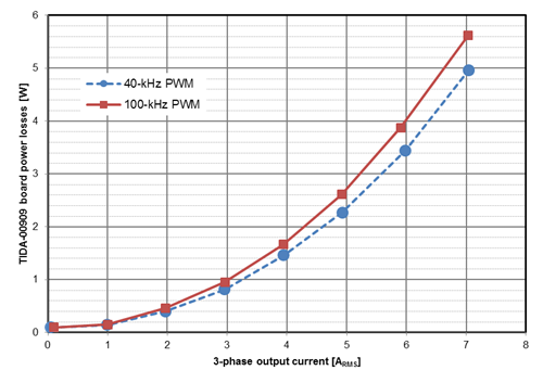
The reference design board’s power losses at a maximum load current of 7ARMS measured 4.95W with a 40kHz PWM frequency, and 5.65W using a 100kHz PWM. Figure 3 shows power dissipation as a function of output current. The theoretical maximum efficiency from the 48V bus is reached at 400W of maximum input power. This gives a phase-to-phase voltage of 34VRMS at a 7ARMS phase current and an inverter efficiency of 98.5% at 100kHz.
 |
|
Figure 3: Gallium nitride reference design power losses at 48V versus three-phase RMS output current. |
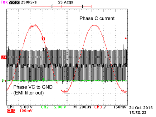
Thanks to the high switching frequency and fast current control loop, the phase current is very close to sinusoidal, shows minimal distortion. This minimizes torque ripple, audible noise while providing the highest efficiency. A plot of the current waveform with the applied PWM voltage is shown on Figure 4.
 |
|
Figure 4: 1kHz sinusoidal phase current shows low distortions with 100kHz PWM. |
We are eager to see what innovative new applications engineers can create by harnessing the power of this exciting new technology.
Additional resources


