Development of scalable perovskite nanocrystals coating technology
Research team at Seoul National University (Prof. Tae-Woo Lee) developed highly efficient large-area perovskite light-emitting diodes (PeLEDs) with an external quantum efficiency (EQE) of 22.5% and pixel size of 102 mm2. The research results were published in Nature Nanotechnology, which is the world-renowned international academic journal, on May 4th (Title: Exploiting the full advantages of colloidal perovskite nanocrystals for large-area efficient light-emitting diodes).
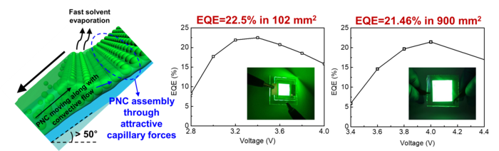
Schematic illustration of the mechanism of the proposed large-area coating method (Left), device efficiency and the photo image of the large-area light-emitting device (100 mm2 (middle), 900 mm2 (Right))
Metal halide perovskites have very narrow spectral emission, excellent color purity, low material cost, and wide and easy color-tunability. Based on these advantages, perovskites are considered as a promising high color purity light emitter which can replace the conventional organic and inorganic quantum dot (QD) light emitters in displays and solid-state lighting technologies. Especially, perovskite is the ever-reported only one emitter which can meet the standard of REC.2020. Therefore, perovskite is expected to contribute to the future ultra-high-definition television (UHD-TV) technology.
Professor Tae-Woo Lee has led PeLED research including the first report of the high-efficiency PeLEDs with EQE of 8.53% in 2015 reported in Science, and EQE 23.4% of the world’s highest efficiency in 2021 reported in Nature Photonics. Subsequently, his research team recently developed the scalable coating method of perovskite nanocrystals to make uniform large-area emitting films and fabricated the highly efficient large-area PeLED with pixel size of 102 mm2 and EQE of 22.5% and reported in Nature Nanotechnology. This EQE value is the highest efficiency in large area PeLEDs (>100 mm2).
Existing high-efficiency, large-area PeLED research were based on bulk polycrystalline thin films. Since the bulk polycrystalline perovskite is simultaneously crystallized during the film formation, the quality of the fabricated PeLED severely affected by the experimental environment and thus the reproducibility is limited. Typically in large-area PeLEDs, it is hard to control the crystal growth to achieve small and fine nanograins. Additionally, spin-coating method which is widely accepted in PeLED research have inherent limitation on uniformity and mass-production of large-area thin film. Therefore, previously reported PeLEDs showed significant efficiency drop in large-area devices.
Professor Tae-Woo Lee and his research team have suggested that the overcoming of the previous intrinsic problems in large-area device can be realized by the use of colloidal perovskite nanocrystals which have a size of several nanometers (1 billionth of a meter). In such a small dimension, charge carriers can be spatially confined to achieve high luminescence efficiency and organic ligands present in the surface of the nanocrystal can effectively suppress the ion migration and charge trapping. Also, highly uniform and reproducible large-area thin films can be achieved with colloidal perovskite nanocrystals which decouples the crystallization of perovskite from the film formation process. Seoul National University research team led by Professor Tae-Woo Lee developed simple modified-barcoating which facilitates the evaporation of residual solvent. PeLEDs that incorporated the uniform modified-barcoated perovskite nanocrystal films achieved EQE of 23.26% and EQE of 22.5% in a large pixel area of 102 mm2 with high reproducibility.
Prof. Tae-Woo Lee said, “This study has developed a technology essential for manufacturing large-area devices, which was the biggest obstacle to commercialization of PeLEDs.” He also commented “It is expected to contribute to the commercialization of PeLEDs by providing the way toward a development of large-scale industrial displays and solid-state lighting that uses perovskites”.
This work was funded by the National Research Foundation of Korea (NRF) grant funded by the Korea government.


