(Author: Skavy Cheng, Editor, LEDinsidehttp:// Translator: Judy Lin, Chief Editor, LEDinside)
According to LEDinside’s latest findings, micro-LEDs will enter mass production by 2018. To understand micro-LED technology comprehensively, and tap into its market potential, LEDinside has organized its history, current situation, theory, manufacturing process, and related manufacturers.
History
The history of micro-LEDs can be traced back to the development of TFT-LCD display backlight module applications, when in the 1990s TFT-LCD developments emerged. Due to the LEDs features in high color saturation, energy efficiency, and in thinness, some manufacturers used the LED as a backlight source. Yet, overtly high costs and poor thermal dissipation, low photoelectric conversion efficiency and other factors, it was not widely applied in TFT-LCD products.
It was not until the year 2000 that white LED chip technology matured, where blue LEDs coated in phosphor powder were excited by electricity to emit white light. By 2008, white LED backlight modules underwent exponential growth, completely replacing CCFL in a short time frame. Leading application sectors included smartphones, tablets, notebooks, table top monitors and TVs.
However, TFT-LCDs are limited by its none-self luminous properties and theory, which caused open cell transmission rate to fall below 7%, causing low photoelectric conversion efficiency in TFT-LCDs. Moreover, white LEDs color saturation performance is much lower than RGB LEDs, hence most TFT-LCD products only have 72% NTSC. Additionally, in outdoor environments a major flaw of TFT-LCDs is its brightness failed to reach above 1,000 nits, causing low image quality and color recognition. Other solutions and developments include using RGB LED as a self-luminous pixel micro LED display.
Current situation
As LEDs mature and evolve, micro-LED display has appeared in a completely new form as of 2010.
From its development history, Sony launched its 55-inch “Crystal LED Display” in 2012, a new micro LED display technology utilizing Full HD Resolution. The display uses about 6.22 million micro LEDs (formula: 1920 x 1080 x 3) for high resolution displays, the contrast ratio can reach 1 million to one, and color saturation of 140% NTSC. The display also does not have reaction time and lifetime issues, but because it uses a single micro LED embedded in the display, there are still a lot of costs and technology barriers to overcome before the product can be commercialized and mass produced.
Although, in theory micro-LEDs can be applied in displays of various sizes, the manufacturing process and yield rates have a negative correlation with display resolution demands. Hence, the products are being introduced into small display applications first, such as wearable devices because of its small size, higher yield rates and high brightness in outdoor environments compared to OLEDs. Additionally, it has low energy consumption.
The average LED chip including substrates and epi-wafer layers measures about 100 to 500 microns (μm), while advanced micro-LED display research is now focused on removing the 4 to 5μm thick LED surface by mechanical or chemical process to transfer the chip onto an IC board.
Micro LED displays combine TFT-LCD and LED technology features, and is a more mature technology in terms of material, manufacturing process, and equipment development than OLED technology. Additionally, micro LEDs product specs are much more advanced than TFT-LCD or OLED, and covers wider applications including flexibility, transparent displays, and is a more feasible next generation display technology.
Starting from 2010, manufacturers have been aggressively developing micro-LED display technology through integration and R&D. Yet, micro LED displays do not have a standardized micro-LED structure, and manufacturers are competing in the fronts of mass production, driver IC design, and aggressively deploying their patent strategies.
As of 2016, manufacturers leading in micro-LED patent applications include Apple affiliated Luxvue, Mikro Mesa, Sony, Leti and others. There are also many companies and research centers that are investing in related technology developments.
Major developers and manufacturers
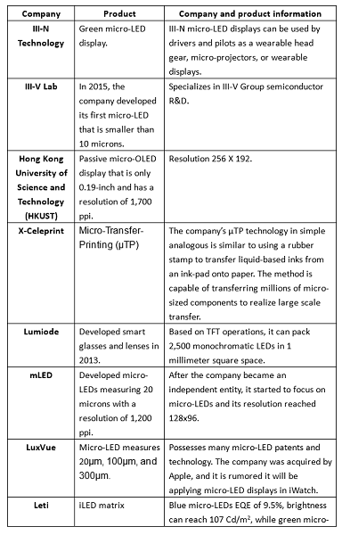 |
 |
|
(Organized by LEDinside) |
Theory
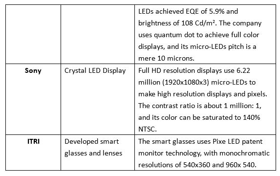
Micro-LED displays in theory is making LED structures thinner, smaller, and in an array structure. Individual micro-LEDs usually ranges from 1 to 10 μm, and are transferred in large volumes onto the IC substrate. The substrate can be hard, flexible, transparent or none transparent. By using physical vapor deposition to complete a protective layer and forming the top electrodes it can be packaged into a simple structured micro LED display.
How to manufacture displays? The LED chip surface has to be placed into an array structure, where each pixel can be individually controlled, and driven to brightness. If the complementary Metal-Oxide-Semiconductor Field-Effect Transistor (MOSFET) will become the main framework for an active micro LED structure, where the micro LED chip array and CMOS can use package technology.
A passive micro-LED structure would adhere the micro-LEDs, a micro lens array could improve the LED brightness and contrast.
 |
|
Micro-LED structure. |
Micro-LED structures
The classical micro-LED structure is a PN junction diode tube made of direct bandgap semiconductor materials, when the micro-LED is forward biased electrons from the semiconductors conduction band recombine with holes from the valence band to release photons that emit a monochromatic colored light. In general, micro-LEDs maximum Full Width at Half Maximum (FWHM) linewdith is 20 nm, and is capable of providing highly color saturation of more than 120% NTSC.
Since 2008, the LED photoelectric efficiency greatly increased to above 100 lm/W, and reached mass production requirements. Hence, micro-LED displays could easily achieve low energy consumption and high brightness designs, due to the display’s self-illuminating properties and simple structure that does not cause any loss of light.
This can solve two major issues in display applications, the first is in wearables, smartphones, and tablet equipment where the displays energy consumption reaches 80%. Display technologies using lower energy consumption could extend battery endurance, while under strong lights in certain environments the displays might create glare, low resolution, while technologies increasing display brightness can be applied to wider range of products.
 |
|
(Organized by LEDinside)
|
Manufacturing methods and technology developments
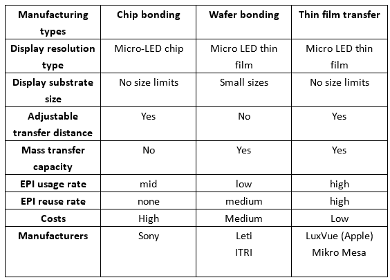
Miniaturization in semiconductor chip processing has reached its ultimate limit, but there is still great room for growth in miniaturization. There are three major production methods for micro-LEDs and can be categorized into chip bonding, wafer bonding, and thin film transfer.
Advantages of each manufacturing process, and companies involved in the manufacturing process.
Chip bonding
By splitting LEDs into micro sized Micro LED chips (including Epi-wafer film and substrate), or using SMT and COB technology, the micro LED chip can be bonded one-by-one onto the display substrate.
Wafer bonding
LED EPI-wafer films will use Inductively Coupled Plasma (ICP) etcher to form a micro grade micro-LED EPI-wafer film structure, once this structure solidifies it will become the display pitch. Once the LED wafer including the EPI-wafer and substrate are directly bonded to the IC substrate, manufacturers will use mechanical or chemical processing to strip away the substrate, leaving the 4-5 micron thick micro LED EPI-wafer film structure that construes the display pixels on the IC driver substrate.
Thin film transfer
Using the mechanical or chemical method to strip away the LED substrate to replace it with a temporary LED EPI-wafer to form a micro-LED EPI-wafer structure. Another method is using Inductively Coupled Plasma (ICP) etcher to form micro-LED EPI-wafer structures, then the substrate is removed using mechanical or chemical methods, and temporarily replaced with another thin film.
Lastly, the display pitch required on the driver IC substrate uses selective transfer fixture to mass transfer the micro-LED EPI-wafer thin film structures to bond onto the substrate and form into display pixels.
Conclusion
Even though Micro-LED displays received large sums of R&D funds, and received attention from leading enterprises, and its specs outshine LCDs, matching OLED picture quality, but at current stage micro-LED displays are still uncommon due to three major barriers:
1) Chip bonding
Take an already mature LED strip light manufacturing process as an example, any flaw or issue in the LED light strip especially embedding millions of LEDs in a display is very difficult technology. While as LCDs and OLEDs are being manufactured through different phases, and has better yield rate performance.
2) Bonding on a LED component.
LED flip-chips are suited for micro-LED display manufacturing, due to its small size, and miniaturization process which does not require metal bonding wire. It can also reduce the gap between LEDs, even though there are still certain issues in the flip chip yield rates, the technology is becoming more comprehensive and has received massive finances. It is also steadily improving.
3) Mass transfer of micro-LEDs.
In the future, the most difficult process in micro-LED displays will be embedded LED process could use mass production methods, especially RGB LEDs present even more difficulties in monochromatic applications. However, in the future as LED adhesives and printing technologies advance, it would be beneficial for micro-LED displays to enter mass production phase.


