 2012-11-02
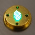
NGK Insulators, Ltd. of Japan has announced the development of high-quality GaN wafers to reduce defects and roughly double the luminous efficiency of green LEDs over previous models. NGK achieved this breakthrough by using a crystal growth technology that it has improved through a proprietary approach. The GaN wafers developed by NGK feature low defect density across the entire 2-inch diameter of the wafer surface and have a colorless transparency. NGK achieved this through proprietary improvements to liquid phase epitaxial technology for single crystal growth. ...
Continue reading →
 2012-11-02


