University of California Santa Barbara (UCSB) in the USA has reported on the use of tunnel junctions (TJs) to stack green and blue micro-sized light-emitting diodes (μLEDs) grown by metal-organic chemical vapor deposition (MOCVD) [Panpan Li et al, Optics Express, vol29, p22001, 2021; Panpan Li et al, Appl. Phys. Lett., vol118, p261104, 2021].
The researchers comment: “The design enables the realization of cascaded blue/green μLEDs in one device with independent junction control, that is, we can control the blue μLEDs, green μLEDs and blue/green μLEDs independently on the same device by injecting current through different pads.”
Normally, such cascaded devices suffer from poor performance since buried p-GaN layers are difficult to realize, particularly in MOCVD. The problem is incorporation of hydrogen from the ammonia (NH3) used as the nitrogen source. Although ammonia is often also used in molecular beam epitaxy (MBE) growth, there is also the potential to use nitrogen gas instead, which avoids the problem. However, MOCVD is the preferred technology in manufacturing due to its faster growth rate, reducing costs and so on.
The incorporated hydrogen passivates the magnesium that is used for p-type doping. Thermal annealing is used to drive out the hydrogen, re-activating the p-GaN. But with buried p-GaN, it is difficult to drive out the hydrogen sufficiently. With μLEDs, however, the sidewall area increases relative to the buried p-GaN volume, potentially allowing efficient escape of hydrogen during annealing.
Tunnel junctions allow current flow through reverse-biased p-n junctions. This is achieved by suitable heavy doping to align the valence and conduction bands of neighboring layers to allow two-way tunneling of electrons and holes through a very thin depletion region.
The team sees potential for cascaded μLEDs from applications such as augmented and virtual reality, large-area displays, and visible light communication systems.
The researchers used standard blue μ
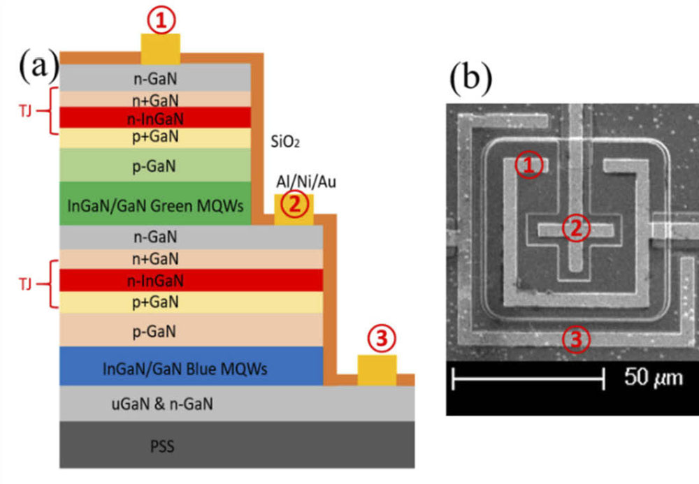
LED wafers as templates for further MOCVD growth of the TJs and green μLED layers (Figure 1). The first TJ consisted of n-InGaN/n+-GaN/n-GaN on the p+-GaN contact layer of the blue μLED structure.
Figure 1: (a) Schematic cascaded TJs blue and green μLEDs and (b) scanning electron microscope image of fabricated device.
The green μLED structure consisted of n-GaN, a superlattice consisting of low-indium-content InGaN/GaN pairs, five InGaN/AlGaN/GaN quantum wells, a p-AlGaN electron-blocking layer, and a p-GaN/p+-GaN contact layer.
The final TJ was grown after removal of the wafer from the reactor and cleaning, followed by return to the MOCVD chamber.
The μLED fabrication began with two reactive-ion etch steps to expose the green and blue n-GaN contact layers. The mesas were small enough to enable rapid thermal annealing (RTA) to drive the hydrogen passivation out of the p-GaN layers through the sidewalls, giving efficient activation of the magnesium acceptors.
Some of the reported μLEDs used indium tin oxide (ITO) as a top contact (Appl. Phys. Lett.) instead of the second TJ (Optics Express). The μLEDs included an omnidirectional reflector layer consisting of five tantalum pentoxide/silicon dioxide pairs and a final aluminium oxide layer, applied using ion-beam deposition. The sidewalls were passivated with atomic layer deposition (ALD) silicon dioxide (SiO2). The ohmic contact metals were aluminium/nickel/gold (Al/Ni/Au).
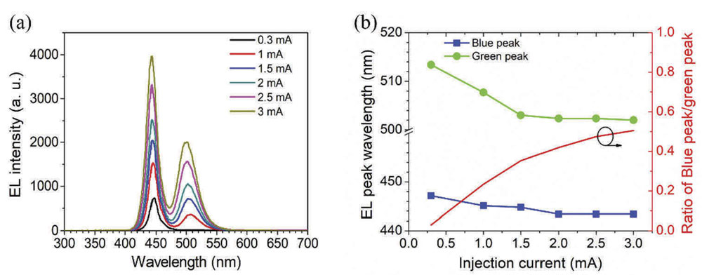
The blue parts of the devices emitted around 450nm wavelength (451nm Appl. Phys. Lett., 455nm, Optics Express).There was some difference in the performance of the green sections: with a top TJ the emissions were towards the blue end at 508nm (0.4mA), compared with 518nm with ITO (3A/cm2). The full widths at half maxima (FWHM) were ~20nm for the blue sections, and ~30nm for the green.
Figure 2: (a) Electrical luminous spectra at various injection currents for blue/green μLEDs with top TJ and (b) extracted blue peak, green peak, and intensity ratio of blue/green peak at various injection currents.
With the top TJ devices the green peak shifted with different injection currents, ranging from 513nm at 0.3mA to 502nm at 1mA (Figure 2). Such blue-shifts are typically attributed to effects such as the filling of higher-energy localized states and charge polarization screening.
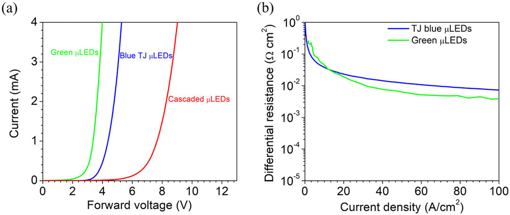
The forward voltages for 1mA current were around 4.2V for the blue section and 3.5V for the green with top TJ. Normalized to the mesa areas, the forward voltage was 4.1V for the blue and 3.1V for the green at 20A/cm2 injection. The researchers see these forward voltages as being among the lowest for green GaN μLEDs with TJ contacts.
Figure 3: (a) Current forward voltage (I–V) characteristics of blue μLEDs, green μLEDs, and blue/green μLEDs with top ITO contact and (b) differential resistance versus current density for blue μLEDs and green μLEDs.
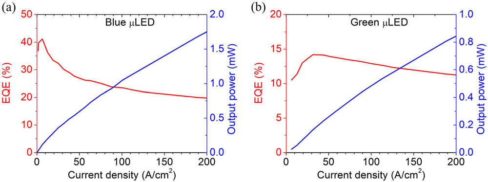
In the devices with top TJ the output power increased linearly up to 4mA injection, reaching 0.89mW for the blue, 0.43mW for the green, and 1.41mW combined.
Figure 4: Output power and EQE versus current density for (a) blue and (b) green μLEDs with ITO contact.
For the devices with ITO contact, the researchers also report peak external quantum efficiencies (EQEs) of 42% for the blue emissions, and 14% for the green. The output powers for these μLEDs reached ~1.8mW blue and ~0.9mW green at 200A/cm2 injection (~7mA blue, ~3mA green), according to the text (the corresponding graphs suggest significantly lower values, which I am following up).