Researchers from the Graphene Flagship use layered materials to create an all-electrical quantum light emitting diodes (LED) with single-photon emission. These LEDs have potential as on-chip photon sources in quantum information applications.
Atomically thin LEDs emitting one photon at a time have been developed by researchers from the Graphene Flagship. Constructed of layers of atomically thin materials, including transition metal dichalcogenides (TMDs), graphene, and boron nitride, the ultra-thin LEDs showing all-electrical single photon generation could be excellent on-chip quantum light sources for a wide range of photonics applications for quantum communications and networks. The research, reported in Nature Communications, was led by the University of Cambridge, UK.
 |
|
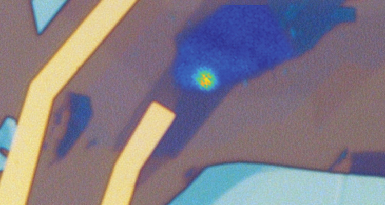
An overlay of the microscope image of a quantum LED device and the photoluminescence image from the active area of WSe2. The isolated bright spot corresponds to a quantum emitter generating a stream of single photons. (Image credit of Mete Atatüre) |
The ultra-thin devices reported in the paper are constructed of thin layers of different layered materials, stacked together to form a heterostructure. Electrical current is injected into the device, tunnelling from single-layer graphene, through few-layer boron nitride acting as a tunnel barrier, and into the mono- or bi-layer TMD material, such as tungsten diselenide (WSe2), where electrons recombine with holes to emit single photons. At high currents, this recombination occurs across the whole surface of the device, while at low currents, the quantum behaviour is apparent and the recombination is concentrated in highly localised quantum emitters.
All-electrical single photon emission is a key priority for integrated quantum optoelectronics. Typically, single photon generation relies on optical excitation and requires large-scale optical set-ups with lasers and precise alignment of optical components. This research brings on-chip single photon emission for quantum communication a step closer. Professor Mete Atatüre (Cavendish Laboratory, University of Cambridge, UK), co-author of the research, explains “Ultimately, in a scalable circuit, we need fully integrated devices that we can control by electrical impulses, instead of a laser that focuses on different segments of an integrated circuit. For quantum communication with single photons, and quantum networks between different nodes – for example, to couple qubits – we want to be able to just drive current, and get light out. There are many emitters that are optically excitable, but only a handful are electrically driven” In their devices, a modest current of less than 1 µA ensures that the single-photon behaviour dominates the emission characteristics.
The layered structure of TMDs makes them ideal for use in ultra-thin heterostructures for use on chips, and also adds the benefit of atomically precise layer interfacing. The quantum emitters are highly localised in the TMD layer and have spectrally sharp emission spectra. The layered nature also offers an advantage over some other single-photon emitters for feasible and effective integration into nanophotonic circuits. Professor Frank Koppens (ICFO, Spain), leader of Work Package 8 – Optoelectronics and Photonics, adds "Electrically driven single photon sources are essential for many applications, and this first realisation with layered materials is a real milestone. This ultra-thin and flexible platform offers high levels of tunability, design freedom, and integration capabilities with nano-electronic platforms including silicon CMOS.”
This research is a fantastic example of the possibilities that can be opened up with new discoveries about materials. Quantum dots were discovered to exist in layered TMDs only very recently, with research published simultaneously in early 2015 by several different research groups including groups currently working within the Graphene Flagship. Dr Marek Potemski and co-workers working at CNRS (France) in collaboration with researchers at the University of Warsaw (Poland) discovered stable quantum emitters at the edges of WSe2 monolayers, displaying highly localised photoluminescence with single-photon emission characteristics. Professor Kis and colleagues working at ETH Zurich and EPFL (Switzerland) also observed single photon emitters with narrow linewidths in WSe2. At the same time, Professor van der Zant and colleagues from Delft University of Technology (Netherlands), working with researchers at the University of Münster (Germany) observed that the localised emitters in WSe2 are due to trapped excitons, and suggested that they originate from structural defects. These quantum emitters have the potential to supplant research into the more traditional quantum dot counterparts because of their numerous benefits of the ultrathin devices of the layered structures.
With this research, quantum emitters are now seen in another TMD material, namely tungsten disulphide (WS2). Professor Atatüre says "We chose WS2 because it has higher bandgap, and we wanted to see if different materials offered different parts of the spectra for single photon emission. With this, we have shown that the quantum emission is not a unique feature of WSe2, which suggests that many other layered materials might be able to host quantum dot-like features as well.”
Professor Andrea Ferrari (University of Cambridge, UK), Chair of the Graphene Flagship Management Panel, and the Flagship’s Science and Technology Officer, also co-authored the research. He adds "We are just scratching the surface of the many possible applications of devices prepared by combining graphene with other insulating, semiconducting, superconducting or metallic layered materials. In this case, not only have we demonstrated controllable photon sources, but we have also shown that the field of quantum technologies can greatly benefit from layered materials. We hope this will bring synergies between the Graphene Flagship and its researchers, and the recently announced Quantum Technologies Flagship, due to start in the next few years. Many more exciting results and applications will surely follow".
Further Reading
-
C. Palacios-Berraquero, M. Barbone, D. M. Kara, X. Chen, I. Goykhman, D. Yoon, A. K. Ott, J. Beitner, K. Watanabe, T. Taniguchi, A. C. Ferrari, M. Atatüre, “Atomically thin quantum light emitting diodes”, Nat. Commun. 7, 12745 (2016). DOI: 10.1038/ncomms12745
-
M. Koperski, K. Nogajewski, A. Arora, V. Cherkez, P. Mallet, J.-Y. Veuillen, J. Marcus, P. Kossacki, M. Potemski, “Single photon emitters in exfoliated WSe2 structures”, Nat. Nanotech. 10, 503 (2015).
-
A. Srivastava, M. Sidler, A. V. Allain, D. S. Lembke, A. Kis, A. Imamoğlu, Optically active quantum dots in monolayer WSe2, Nat. Nanotech 10, 491 (2015)
-
P. Tonndorf, R. Schmidt, R. Schneider, J. Kern, M. Buscema, G. A. Steele, A. Castellanos-Gomez, H. S. J. van der Zant, S. Michaelis de Vasconcellos, R. Bratschitsch, “Single-photon emission from localized excitons in an atomically thin semiconductor” Optica 2, 347 (2015)


