 2013-03-22
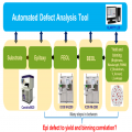
Author: Steven Chen, Process Control Solutions Technologist, KLA-Tencor Corporation Introduction LED manufacturing is undergoing a tremendous transformation. The evolution to high brightness LED, larger wafer size and new complex architectures make LED manufacturing more challenging than ever before. Even though these trends greatly benefit the advancement of the LED industry in terms of LED efficiency and performance, they can also potentially negatively impact yield. In order for LED manufacturers to stay competitive in this dynamic environment, they need to have a comprehensive in-line process control strategy to improve the yield to make the solution cost effective. Currently, most LED manufacturers rely on inspection tools to inspect and provide defects of interest (DOI). Defect density is typically utilized as the gauge for statistical process control (SPC) control. However, the drawback of this approach is the fact that there can potentially be a lot of nuisance defect that does not cause yield loss. In looking at a defective wafer through an inspection tool, how do you determine which defects are killer defects that impact the yield or electrical performance, and which defects are nuisance? How can killer defects be detected at the earliest possible time to prevent costly excursions? These are the questions that must be addressed properly.
Continue reading →
 2013-03-22


