(Author: Judy Lin, Chief Editor, LEDinside)
The LED industry is hunting for innovative technologies and application fields, as lighting and backlight market growth wane. UV LEDs over the past year has caught many LED manufacturers attention, the budding UV-A LED market application sector in nail curing, air purification, and printing applications is attracting top LED players including Nichia and Osram to invest in the sector. UV-C LED or DUV LED that has a wavelength ranging from 200 nm to 280 nm remains a market sector that barely exists at the moment, due to certain technical challenges that call for new solutions.
UV LED market is gaining traction, as industry insiders note the Minamata convention to phase out all mercury based lamps by 2020 will offer large growth potential, since most UV lights on the market are still mercury-vapor lights. However, it has been difficult for companies relying on visible LED chip structures to make efficient DUV LEDs in the 260 nm wavelength, which is the most effective range for destroying DNA in virus and bacteria in sterilization applications.
 |
|
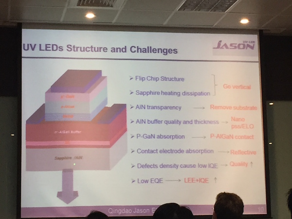
Jason Electric presentation shows challenges in current DUV LED designs using visible LED chip structures. (All photos courtesy of LEDinside) |
Current challenges in DUV LED chip designs
Low internal quantum efficiency (IQE) caused by high lattice mismatch between sapphire substrate and aluminium nitride (AlN) template used to make UV LEDs, lack of good encapsulent materials, improving thermal dissipation and UVC LED lifetimes are some of the issues manufacturers still need to overcome, said James Wu, Vice President, Qingdao Jason Electric during IR+UV Summit organized by SEMI on Thursday.
Using sapphire substrate based blue LED manufacturing methods, the IQE is usually below 20% internal quantum efficiency (IQE) in DUV LED applications compared to 50% to 60% in blue LEDs, while the external quantum efficiency (EQE) is about 8%, said Wu.
The main cause of the low IQE is high lattice mismatch between sapphire and AlN, where the defect rate is much larger compared to blue LEDs. One solution to get around the loss of light from lattice defects is growing thicker AlN buffer layers, which at best brings defect density to 109 cm2.Although, the large defect density can be significantly lowered to 105 cm2 by switching to bulk AlN substrate, the material is simply too costly at the moment, explained Wu.
 |
|
James Wu, Vice President, Qingdao Jason Electric. |
UV LEDs are typically driven at higher power to reach the desired wavelength output, which makes thermal dissipation an important aspect of the chip design. Yet, sapphire is not a very good thermal conductor, which makes it difficult for the chip to dissipate heat, said Wu. High temperatures will shorten the LEDs lifetime. Leading DUV LED maker Nikkiso has reached 10,000 hour lifetime milestone, which is still about half the lifetime of visible light LEDs that on average have at least 20,000 hours lifetime.
Encapsulent is another area where blue LED manufacturing methods are not directly transferrable to UV LEDs, according to Wu. Flip chip structure UV LEDs already present considerable challenges, but there is currently not any reliable or suitable silicone resins for UV LED applications. QD Jason, a Chinese UV LED manufacturer which has been in the UV LED industry for more than 10 years, is studying fluorine resins at the moment, said Wu. Encapsulents remain important in the DUV LED design, without it the chip would lose 1.5 times its power, he added.
QD Jason is aiming to mass produce 5-20 mW DUV LEDs in 2016, and has achieved 176 mW at 1 Amp (A) current in lab conditions. The company is currently focusing on low to mid power DUV LED applications and diversifying its product range. Leading Japanese DUV LED manufacturer Nikkiso is mass producing 50 mW at 350 milliamp (mA) DUV LEDs in 2016.
 |
|
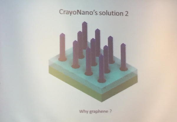
A 3D rendered image of CrayoNano's nanorods grown on graphene. |
Nanorod LEDs grown on graphene a potential solution for DUV LEDs
Taking into consideration the numerous challenges of growing DUV LEDs on sapphire, Norwegian startup CrayoNano proposes to grow nanorod structure LEDs on graphene to solve efficiency issues.The company was spun-off from Department of Electronics and Telecommunications at the Norwegian University of Science and Technology (NTNU) in Trondheim holds 9 different patent families for semiconductor nanowire on graphene. The research institute specializes in III-V group nanorod research applicable in solar cells and LEDs prior to transiting into LEDs.
UVC LEDs currently do not use transparent substrates, the p-GaN cap absorbs a lot of light. UVC LEDs is also largely absorbed by the substrates, said Dr. Helge Weman, Founder and Chief Technology Officer, CrayoNano. The use of AlGaN on sapphire in DUV LED applications causes difficulties in thermal dissipation, since most of the chip’s energy is converted into heat instead of light, said Weman.
 |
|
Dr. Helge Weman, Founder and Chief Technology Officer, CrayoNano. |
An alternative solution is growing nanorod structures on transparent graphene substrates, since nanorods are less sensitive to lattice mismatch. Still in the R&D phase, CrayoNano’s research found AlGaN’s low lattice mismatch with graphene is mere 2% making the atomic thin and flexible material an ideal substitute for sapphire. Research conducted by McGill University also showed significant advantages of growing nanorod LED structures on silicon, showed IQE reached 80%.
Asked about the high costs of graphene, Weman pointed out prices were falling to levels matching silicone wafers. He also pointed out AlN materials are just as expensive, and would make little difference for DUV LED manufacturers. Equipment manufacturers including Aixtron are also making machines for manufacturing 8-inch graphene wafers, but until a large application market emerges prices will probably not decline at a rapid pace for graphene yet.
The next phase for CrayoNano is making prototype DUV LED dies that can be shipped to LED manufacturers, and forming partnerships in this sector. Even though this is a relatively new concept, experimenting with new substrate and LED chip structures might be urgent for companies aiming to mass produce UVC LEDs by 2020.


