Germany-based IP licensing company ALLOS Semiconductors sees itself as the leading provider of GaN-on-Si wafer technology for LED, power and RF applications and claims to have the best performance in the market with respect to essential properties like crystal quality, uniformity, and low wafer bow.
LEDinside had a chance to sit down face to face with Burkhard Slischka, CEO of ALLOS, to talk about the company’s proprietary technology and his vision for the future of micro LED.
 |
|
(Image: ALLOS Semiconductors) |
Q: Burkhard, glad to have you here. Let’s start with the question many readers have: Why GaN-on-Si? Almost all conventional LED production is on sapphire. Why should that be different for micro LEDs?
A: For a successful production of micro LEDs fundamental changes are needed. New device designs and novel manufacturing techniques are to be used and – most importantly – production yield has to be brought to a level far better than anything the LED industry has seen. For all these changes GaN-on-Si is a key enabler and saves cost.
Q: So moving to GaN-on-Si is all about better yield and cost in your opinion?
A: Yes, exactly. And to understand this we need to look at the entire value chain from growing the epiwafer until the micro LED chips are successfully build into the display.
Q: On this value chain, where do you see the biggest impact by using GaN-on-Si?
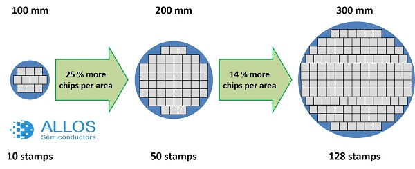
A: We see three factors along the entire chain: the cost advantages of bigger wafer diameter, the advantages of silicon for thin film processing and the huge influence of wafer uniformity on yield.
Q: Let’s start with uniformity. End of 2017 Veeco and ALLOS made a joint press release claiming that your technology has achieved the best uniformity published for 200 mm GaN-on-Si. How does this compares with GaN-on-sapphire?
A: We showed a standard deviation for emission wavelength of below 1 nm. Other uniformity values like thickness are even better. These values for 200 mm GaN-on-Si compare very well with 150 mm GaN-on-sapphire. Especially as our technology has very good wafer-to-wafer reproducibility.
“The next target is to have 99 % within a +/- 1 nm bin”
Q: Do you see room for further improvement?
A: Yes, we certainly do. We achieved these results after only four weeks project work on Veeco’s Propel reactor. So there is still a lot of room for improvement. The next target is to have 99 % of the wafer area within a +/- 1 nm bin.
Q: Are you saying that you can get the same or even a much better uniformity on 200 mm GaN-on-Si compared to what others can achieve on 150 mm GaN-on-sapphire?
A: Correct, same uniformity, but on a wafer area almost twice as big.
Q: It seems having excellent uniformity is of much higher importance than for conventional LEDs. Why is that?
A: Uniformity is the essential enabler for yield. For every display you need millions of micro LED chips with precisely the same wavelength. Sorting LED chips before assembly or any pixel repairing afterwards is driving up the cost of the display. Therefore, this issue must be solved right at the beginning with very uniform epiwafer material, otherwise micro LED displays will not be cost competitive.
Q: In this context, what is more important in your opinion, having the best wafer uniformity or the lowest epi cost per wafer area?
A: Good question. Looking at one of the two items alone is short-sighted. A wafer with better uniformity drives up yield in all following manufacturing steps. So even if the epi cost would be higher, it can easily be over-compensated by the cost savings resulting from the better yield.
“Using 200 mm CMOS saves 45 %”
Q: Which leads us to the second factor you mentioned before, the cost advantages of bigger wafer diameter. I understand that moving to larger wafer diameters is driving down cost per chip. But wouldn’t that be the same for 200 mm GaN-on-sapphire?
A: Yes, in principle one should think so. Except that there are three problems for sapphire: 1) The high cost of 200 mm sapphire substrates, 2) It might be impossible to achieve the needed wafer uniformity and 3) to get to sufficient manufacturing yield due to strong wafer bow. But even more important is another advantage of GaN-on-Si: You can use existing 200 mm CMOS processing capacity and expect a cost saving per area of 45 %. At the same time, it offers the high processing yield needed for micro LEDs which conventional LED sites could match only after massive CAPEX and skill upgrades.
Q: And the 45 % you mentioned is only from chip processing?
A: Right, there are more contributions coming from higher yield at substrate removal and bonding and better area economics at mass transfer.
Q: There is one more technical argument I would like to understand. How can you achieve the uniformity target on 200 mm on silicon while it is so difficult on sapphire as you are saying?
A: Our GaN-on-Si technology comes with a unique strain engineering technology. This allows us to achieve two things at the same time: We can have very good temperature homogeneity during growth – enabling the uniformity we talked about before – and a flat and crack-free wafer after cooling down. Usually these two items are seen as trade-offs, but we can provide both. And by the way, we are very confident to scale this even to 300 mm.
“Flat and crack-free 300 mm is possible”
Q: 300 mm GaN-on-Si?
A: Yes, 300 mm is possible. Unfortunately, there is no industry-grade MOCVD equipment for 300 mm available yet. But we are optimistic that this will change and we can demonstrate the first flat and crack-free 300 mm GaN-on-Si epiwafer soon.
Q: Very interesting! I got the cost advantages of GaN-on-Si for micro LEDs you just described. But what about performance differences to GaN-on-sapphire? From what we hear there are concerns in the industry about brightness and light efficiency on GaN-on-Si.
A: In fact, it is very difficult to achieve good enough crystal quality with GaN-on-Si and this damages the LED performance as you mentioned. We overcame this limitation and have the best crystal quality on GaN-on-Si in the industry. Actually, our top layer defect density is only 2 x 108 cm-² TDD which is on pair with the value on sapphire.
Q: What does that mean in terms of LED performance?
A: It means that once we have licensed and transferred our technology to a customer their existing light emitting layer as they grow them today on sapphire and our GaN buffer on silicon will be integrated into one recipe. This results in a GaN-on-Si wafer with all the superior properties we have already talked about and also with the same light emitting structure and performance our customers have today on sapphire.
“Same performance as on sapphire”
Q: Let’s move on to the business side. How will the supply chain look like for micro LEDs?
A: The target applications of the large device makers will determine development and business decisions. Either the device makers for smartphones, TVs or other kinds of gadgets will follow Apple’s example and built up micro LED capabilities in-house. Or they incentivize strategic partners to provide solutions for parts along the value chain. But in either case they need to coordinate technology, yield and cost along the value chain and finance to a certain degree the development. Just to wait for some supplier to provide the end-to-end solution for micro LEDs does not look like a viable strategy to me.
Q: How will that impact ALLOS’ future business strategy?
A: ALLOS has strong GaN-on-Si technologies for three markets, LED, power and RF. We see that these three markets require different technology and business set-ups and that we also need to apply different strategies and strategic partnerships in these three markets.
Q: What are your objectives in micro LEDs in the next two years?
A: In micro LEDs we are engaged with big corporations and start-ups alike to further develop the technology. We see that we are in a strong position based on the excellent performance we have already today and our solid IP portfolio. Now it is equally important to have the other right partners along the value chain and the needed funds to develop micro LEDs into production readiness.
Q: If I were one of the large device makers you mentioned before and would lead and sponsor such development I would demand to get exclusive rights on the developed technology too…
A: Yes, we hear this argument a lot these days and with the right set-up this might be a win-win solution.
Q: Thanks for talking to us, Burkhard. See you in July at our micro LED forum!
A: I am looking forward to it!


