Panasonic Corporation announced today that it has developed the industry’s smallest*1 semiconductor device, the “PhotoMOS”[1] CC type series, which achieves low consumption current and contributes to equipment downsizing. The relay is operated with a low consumption current, and as a result the working time of the battery operating the equipment is longer. It enables steady operation for measuring equipment, probe cards [2], wearable devices, security equipment and medical equipment.
The PhotoMOS CC type series will be shipped in May 2015.
*1: As a semiconductor-type relay with MOS FET on the output side.
As of May 8, 2015, according to a survey by Panasonic.
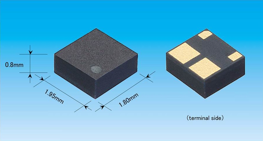
Owing to increasing semiconductor density and greater on-chip integration, chips are being made with many more pins. Since a relay is needed to measure current and voltage on each pin, demand has been growing to keep down the size of IC testers, probe cards, and other measuring equipment. Meanwhile, it is also imperative to minimize consumption current in order to extend the battery life of equipment such as wearable devices and security equipment, and medical equipment that include a high number of relays. Panasonic has succeeded in creating the industry’s smallest*1 (1.8 × 1.95 × 0.8 mm) “PhotoMOS” CC type, which also boasts a low consumption current (0.2mA). Panasonic’s unique feature capacitor couples isolation[3] with a small size and a low consumption current. It can operate in high operating temperatures (up to 105°C) and can be used in equipment designed to operate in high temperature environments.
 |
|
Industry's smallest semiconductor-type relay "PhotoMOS" CC type (Panasonic/LEDinside) |
Features
1. Industry's smallest *1 size. It will contribute to equipment downsizing.
D 1.8 × W 1.95 × H 0.8 mm: 46% smaller mounting area than our previous product*2.
2. Low consumption current. It will contribute to more energy efficient equipment.
Input current, 0.2mA: Our previous product*2, 5 mA
3.
Guaranteed performance at high temperature. It will contribute to equipment with higher performance under higher temperatures.
Operating temperature, –40℃ to +105℃: Our previous product*2 ,–40℃ to +85℃
*2 Compared with Panasonic’s previous product , part number AQY221R2M (D 2.95 × W 2.2 × H 1.4 mm)
Applications
-
Small form factor measuring equipment requiring high density mounting.
-
Low consumption current wearable devices and battery operating equipment.
-
Measuring equipment requiring good high temperature performance.
Explanation of key features
1. Industry's Smallest *1 size. It will contribute to equipment downsizing.
Panasonic has applied our accumulated expertise with fine processing technology to equip our “PhotoMOS” with optical isolation[4], but now we have implemented capacitor coupled isolation. By adopting a capacitor coupled isolation driver[5] on the input side, it has been possible to overcome the obstacles to downsizing that were encountered with optical isolation. Using the industry’s smallest (1.8 × 1.95 × 0.8 mm) TSON[6] package, it is now possible to design smaller, higher performance probe cards and other measuring equipment.
2. Low consumption current. It will contribute to more energy efficient equipment.
Panasonic’s new “PhotoMOS” CC type features proprietary, newly developed capacitor coupled isolation drivers. It achieves low consumption current operation, now 0.2mA, which our previous models with optical isolation could not manage. Greater energy efficiency also contributes to greater service lifetime for equipment that incorporates lower power consumption.
3. Guaranteed performance at high temperature. It will contribute to equipment with higher performance under higher temperatures.
Along with the anticipated rising demand for automotive semiconductor devices, which have to work in harsh environments, users want probe cards and other measuring equipment to be capable of carrying out measurements in hot conditions. In previous products, optical isolation technology was a bar to high temperature operation, however, with their specially developed capacitor coupled isolation drivers, these new “PhotoMOS” are guaranteed to operate at up to 105°C and enable design of equipment with improved heat performance.
Notes
[1] “PhotoMOS”
General term for a semiconductor-type relay that implements isolation of the input side and output side using a device to control current ON/OFF. A MOSFET (switching element) is used on the output side. PhotoMOS is a trade name belonging to Panasonic.
[2] Probe card
An electrical/mechanical part of equipment used during semiconductor manufacturing. Since devices have been getting faster, their capacity larger, and more complex, there has been demand for better performance and downsizing.
[3] Capacitor coupled isolation
A relay consisting of a semiconductor device with MOSFET on the output side, and use of a driver IC (comprising a driver circuit) on the input side.
[4] Optical isolation
A relay consisting of a semiconductor device with a MOSFET (switching element) on the output side, and use of an LED and light-receiving element on the input side.
[5] Capacitor coupled isolation driver
This refers to the input isolation element comprising an isolation capacitor and peripheral circuitry made using our unique technology. This enables downsizing, consumption current reduction, and better heat performance than the previous product that used an LED for optical isolation.
[6] TSON
Panasonic’s unique package type: short form for “Thin Small Outline No lead”.
Product Inquiries
http://www3.panasonic.biz/ac/e/control/relay/photomos/cc/cc1a_aqy2c_r_cr/index.jsp
AIS company Inquires
http://www.panasonic.com/global/corporate/ais.html


