2015-05-12

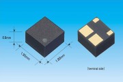
Panasonic Launches Industry's Smallest Semiconductor Device 'PhotoMOS' with Low Consumption Current

Panasonic Corporation announced today that it has developed the industry’s smallest*1 semiconductor device, the “PhotoMOS”[1] CC type series, which achieves low consumption current and contributes to equipment downsizing. The relay is operated with a low consumption current, and as a result the working time of the battery operating the equipment is longer. It enables steady operation for measuring equipment, probe cards [2], wearable devices, security equipment and medical equipment.
Continue reading
ALLOS Semiconductors of Germany and Ennostar Corporation of Taiwan today announced a strategic partnership to bring 200 mm GaN-on-Si (gallium nitride on silicon) LED epiwafers for microLED applications into volume production. This collaboration r... READ MORE

The Fighting Illini turned to Daktronics (NASDAQ-DAKT) of Brookings, South Dakota, to design, manufacture and install the largest main video display in college football, totaling 17,300+ square feet. The project includes 16 LED displays that c... READ MORE