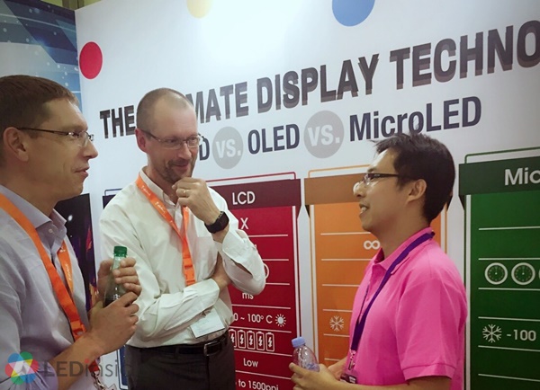
At Semicon Taiwan 2017, PlayNitride showcased both single-color and multi-color transparent Micro LED displays for wearable devices and game consoles. With a transparency level up to 50%, those displays, once upsized, can be used on more applications, which possibly leads the market of Micro LED to enlarge. On the other, in response to clients’ needs for fine-pitch LED displays, PlayNitride also gets Mini LED under development. Its Mini LED displays as of now are able to reach P 0.75 (0.75 mm per pixel pitch). The company attempts to develop Micro LED displays of larger sizes and anticipates to roll out its innovations in 2018 at the earliest.
 |
|
(Image: LEDinside) |
PlayNitride expressed a difficulty in the binning process that the micron-sized chips are too small to be properly grouped, inspected, and repaired. Meanwhile, it has to make sure the quality of epitaxy for the chips meet the stringent standards: high uniformity, zero defects/ zero particles, and decent thickness. In addition, manufacturers have to control the external quantum efficiency of the chips and tackle leakage issues. After attaining all these, companies can really reduce the production cost by enlarging the display size.
 |
|
(Image: LEDinside) |
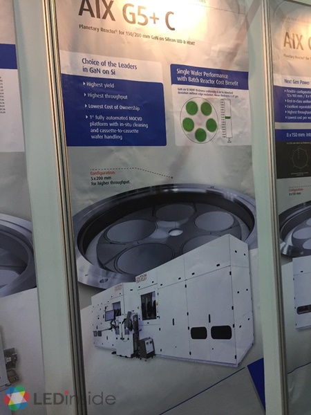
AIXTRON, the noted German MOCVD provider, promoted that its AIX G5+ C system can produce wafers that achieve sizes of over 8 inches, minimum defects (10-20 particles), and high wavelength difference with a difference of ±1nm. Alan Tai, General Manager at AIXTRON, told LEDinside they already received several orders and offered the system to their clients. Being able to produce wafers meeting industrial standards is the selling point capturing clients’ hearts. The system is likely to play a crucial role in the industry after Micro LED starts to take off.
 |
|
(Image: LEDinside) |
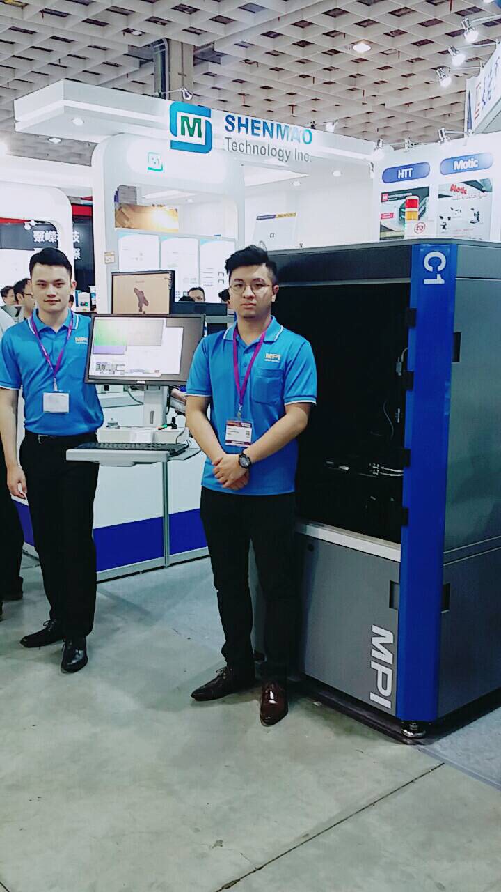
MPI Corporation also develops wafer bonding and testing equipment to contribute to the production. The MPI C1 system featuring electrodes in the size of 40x15µm is able to inspect both optical and electric parameters of wafers. It is now available for ordering.
(Author: Joanne Wu of LEDinside)


