More and more companies, big and small, have utilized their self-developed methods to produce Micro LED products, whether they are Micro LED TVs, display modules, head-up displays (HUDs), or microdisplays. Through numerous collaborations between LED manufacturers and equipment providers, the production of Micro LED chips started to slightly increase. Research institutions have been trying to realize their ideas, trial after trial, to improve mass transfer technologies. As for young startups, they also devised several intricate technologies that can effectively address some of the technology barriers, which is attractive enough to get them helpful partners.
JBD, a HK-based startup founded in 2015, carried out extensive research and development work to realize inorganic compound semiconductor material based display technology. Near the end of 2017, JBD introduced a new Micro LED technology for microdisplay manufacturing. LEDinside contacted Dr. Fang Ou, CTO, and Dr. Lei Zhang, CEO of JBD, and got the information about the technique in detail.
Flip-chip Technology vs. Hybrid Integration Technology
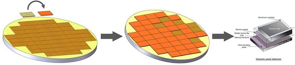
At present, among Micro LED developers, the most universal approach to produce Micro LED microdisplays is the flip-chip technology, said Dr. Zhang. Basically, they manufacture two wafers, one of which carries a layer of light emitter and the other the IC driver. Then, the wafer which carries Micro LEDs is diced into separate chips and flip-bonded on to the wafer with IC driver via solder bonding.
 |
|
(Image: JBD) |
This common manufacturing technology when producing micron-sized LED chips induces a few issues, such as coefficient of thermal expansion (CTE) mismatch, alignment accuracy problems, and device reliability issues. Under the situation that every process is at a microscopic level, difficulties of managing different thermal expansion rates between different materials and maintaining high alignment accuracy of Micro LED chips and the IC driver while bonding surely rankle those firms. They are grasping at straws to find solutions or adjust techniques to solve these challenges.
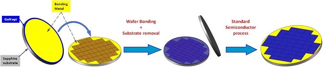
However, JBD’s R&D team successfully sidestepped those challenges with a technology they devised and have patented—the wafer scale monolithic hybrid integration technology, Zhang confirmed with a confident tone. The general concept of the technology is to transfer functional Micro LED epitaxial layers onto silicon IC wafers. The team firstly bonds a Micro LED epi-wafer to the IC wafer and then removes the Micro LED growth substrate, making the process a blank epi-layer transfer to integrate Micro LED epi-layers with a corresponding silicon IC wafer.
 |
|
(Image: JBD) |
With one substrate as a base, the two materials are bonded together and become an epi-on-IC structure that is then subject to subsequent wafer-level semiconductor fabrication processes to produce monolithic hybrid integrated Micro LED chips. Instead of having two substrates in the structure, the technology simplifies it leaving only one substrate within.
For JBD that mainly focuses its Micro LED development on applications such as near-eye wearable devices for AR and HUDs, the technology pays off significantly, most notably in terms of pushing down the pitch size of its Micro LED microdisplays, explained Dr. Ou. Without sacrificing the image quality and system compactness, display panels for AR applications need to have very fine pitches to achieve desired high resolution. The pitch might need to be as small as 5µm or even smaller. With the technology, JBD dodges the process to bond pre-defined Micro LED arrays to the driver ICs, during which aforementioned problems would happen to make downsizing the pitch size more difficult.
Goal for 2018-2019: Push Down Display Size by 50% While Keeping High Resolution
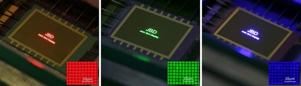
At the beginning of 2018, JBD demonstrated active matrix Micro LED microdisplays in red, green, and blue. According to Zhang, those monochromatic displays are sized 12.8mm in length, 9.6mm in width and are composed of Micro LEDs with a device size of 2-3µm. Manufactured with the monolithic hybrid integration technology, they feature a pitch size of 5µm. The high pixel density grants an ultra-high resolution of higher than 5,000ppi.
 |
|
(Image: JBD) |
Ou revealed that currently the yield of Micro LED pixels on a final microdisplay made by JBD has already surpassed 99.99%, a percentage that is still very hard for other incumbent technologies to attain right now considering the size and volume of the pixels. Now here, if we take that number as a message saying that the chance of those Micro LED displays needing a repair is low, JBD sounds very likely to get the production cost of its displays under a certain level of control by potentially saving quite a bit on costly repairs. The startup will continue to enhance the quality of its epitaxy and improve the integration process in hope to push the yield high enough to hit the requirement for mass production, continued Ou.
Finished prototype wise, Ou also said that around the beginning of 2019 the company will introduces a few more Micro LED displays with finer specifications. The displays to be launched are expected in only half the size of their predecessors. Their pitch size will be refined to be 2.5µm and the size of each pixel will only be 1.5-1.7µm, whereas the resolution will go up to 10,000ppi.
In addition, JBD is also working on the color conversion of its Micro LED microdisplays for near-eye projection. “We are developing technologies for color conversion of the displays. There are essentially two approaches—one using external optics and the other with the hybrid integration technology,” said Ou. “For the later approach, we are attempting to use the technology to transfer blank red, green, and blue Micro LED epi-layers together onto the driver ICs. Vertically aligned, those light-emitting layers, along with the driver ICs, will form a 3D structure. Depending on the LED materials, the driving voltage will be controlled in the range of 3.3V-5V.”
The startup has been teaming up with its customers to develop competitive products for the wearable device and automotive display markets. Apart from high resolution, high brightness is another requirement for such applications, stressed Ou. The company aims to raise the brightness of its products to be higher than 100,000 nits, which ensures the quality of images under strong outdoor ambient light (5,000-8,000 nits). “We are seeking more strategic partnerships to upgrade our products and make the commercialization of Micro LED-based devices as soon as possible,” concluded Ou.
(Dr. Fang Ou and Dr. Lei Zhang from Hong Kong Jade Bird (JBD) were interviewed by Simon Yang, Max Chen, and Evangeline Huang. The article was written by Evangeline Huang, Editor, LEDinside.)


