Osram Opto Semiconductors is keeping pace with the constant growth of the market and switching its fabrication of red, orange and yellow light emitting diodes to 6-inch wafers. The German high-tech company is therefore extending the fabrication of all large-wafer LEDs to the indium-gallium-aluminum-phosphide (InGaAlP) material system and therefore expanding its production capacity. The company began switching fabrication of blue LED chips back in 2011.
The latest switch involves chips for LEDs intended for an extremely wide range of applications. Red and yellow LEDs are used in virtually every sector: as turn indicators, brake lights and interior vehicle lighting in the automotive sector, in displays, for projection, for signage and for color mixing systems in general illumination. Osram Opto Semiconductors is one of the pioneers in switching production. The Regensburg based company was the first manufacturer to switch all LED colors worldwide to 4-inch wafers many years ago and is now continuing this approach with 6-inch wafers.
 |
|
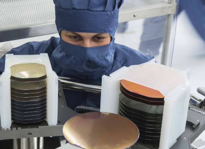
A view of the clean room: The assembly system transporting a 6-inch wafer; 4-inch wafers can be seen on the left. (LEDinside/Osram) |
Continual market growth
“The demand for light emitting diodes in red, orange and yellow continues to grow. We are keeping pace with this demand by being the first manufacturer in the world to switch fabrication to 6-inch wafers – thereby also expanding our capacity", said Aldo Kamper, CEO of Osram Opto Semiconductors. “The switch will involve all product families and was initiated at the start of the year”, he added. The red, yellow and orange chips will be fabricated at the company headquarters in Regensburg. InGaN chips for blue, green and white LEDs are also produced there, as well as in Penang, Malaysia.
Osram as an innovation driver
Experience from 6-inch wafer production so far has flowed directly into the current process – as have the results from the projects funded by the German Federal Ministry of Education and Research (the “GallEff” project and the “Greight” project for scaling indium-gallium-nitride wafers). Osram Opto Semiconductors is therefore pursuing its platform strategy and is already looking to the next stage in development as part of its research activities, namely even larger wafer diameters and alternative substrates. Highly promising projects are already under way in the laboratories of the high-tech company and in other more general funded projects. Osram Opto Semiconductors is therefore demonstrating its powers of innovation not only in product developments but also in production technologies and processes.


