Long-term collaboration for growth of 6-inch GaN-on-Si wafers planned
AIXTRON SE today announced that the University of Cambridge has successfully commissioned another multi-wafer Close Coupled Showerhead (CCS) MOCVD reactor at its new facility at the Department of Material Science and Metallurgy. The CCS 6x2-inch system will be configured to handle single 6-inch (150mm) wafers (1x6-inch).
“We will be using the systems to expand our research efforts for LED and electronic devices based on gallium nitride (GaN) epitaxy on 6-inch silicon wafers,” comments Professor Sir Colin Humphreys, Director of Research in the Department of Materials Science and Metallurgy. “We already use one CCS 6x2-inch system in our work, but the gathering pace of GaN-on-Si development means that we need an extra system with large diameter wafer handling.”
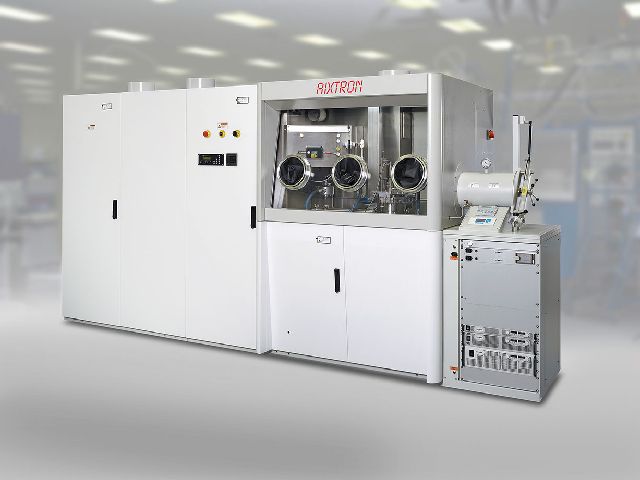
Tony Pearce, Managing Director at AIXTRON Ltd., comments: “AIXTRON is proud to continue its long-standing collaboration with the University of Cambridge and to supply another state-of-the-art CCS research system to complement the university’s existing reactor. Under Prof. Humphreys’ lead, the Cambridge group has developed world leading GaN-on-Si processes and we look forward to further supporting this work with this new system.”
Dr. Frank Schulte, Vice President AIXTRON Europe, adds: “We are very pleased to announce this repeat order from Prof. Colin Humphreys and his team, pioneers of the GaN-on-Si technology, as they push the industry forward to success. Using silicon substrates for power electronics and LED applications, this technology should gain a big share from the existing market.”
The Centre for Gallium Nitride inCambridge,UK, not only grows nitride semiconductors, but is one of the few places in the world to have on the same site extensive advanced characterization facilities such as electron microscopy, X-ray diffraction, atomic force microscopy, photoluminescence (PL), and Hall effect equipment. The team also includes specialists in basic theory for understanding in detail the physical properties of nitride semiconductor materials.
AIXTRON SE today announced that the University of Cambridge has successfully commissioned another multi-wafer Close Coupled Showerhead (CCS) MOCVD reactor at its new facility at the Department of Material Science and Metallurgy. The CCS 6x2-inch system will be configured to handle single 6-inch (150mm) wafers (1x6-inch).
“We will be using the systems to expand our research efforts for LED and electronic devices based on gallium nitride (GaN) epitaxy on 6-inch silicon wafers,” comments Professor Sir Colin Humphreys, Director of Research in the Department of Materials Science and Metallurgy. “We already use one CCS 6x2-inch system in our work, but the gathering pace of GaN-on-Si development means that we need an extra system with large diameter wafer handling.”
Tony Pearce, Managing Director at AIXTRON Ltd., comments: “AIXTRON is proud to continue its long-standing collaboration with the University of Cambridge and to supply another state-of-the-art CCS research system to complement the university’s existing reactor. Under Prof. Humphreys’ lead, the Cambridge group has developed world leading GaN-on-Si processes and we look forward to further supporting this work with this new system.”
Dr. Frank Schulte, Vice President AIXTRON Europe, adds: “We are very pleased to announce this repeat order from Prof. Colin Humphreys and his team, pioneers of the GaN-on-Si technology, as they push the industry forward to success. Using silicon substrates for power electronics and LED applications, this technology should gain a big share from the existing market.”
The Centre for Gallium Nitride inCambridge,UK, not only grows nitride semiconductors, but is one of the few places in the world to have on the same site extensive advanced characterization facilities such as electron microscopy, X-ray diffraction, atomic force microscopy, photoluminescence (PL), and Hall effect equipment. The team also includes specialists in basic theory for understanding in detail the physical properties of nitride semiconductor materials.


